
Programable Board with 32K RAM

More: The only components necessary to extend the RAM are a 32k static RAM chip, an octal latch for some of the address bits, and the necessary decoupling capacitors. The 0.33 µF caps I used are tantalum, and the RAM I used has 150 ns access time. In the schematic above, I connected any address line from the controller or the latch to any address line on the RAM chip. Similarly, any data line from the controller can connect to any data line on the RAM chip. This makes wiring of the board (or layout of the PCB) simpler than trying to connect corresponding address and data lines.
The circuit described involves the integration of a 32k static RAM chip, specifically the Cypress CY7C199-150, into an existing system to enhance memory capabilities. The primary objective is to expand the program memory to accommodate additional features such as EEPROM support, increased stack space, and advanced data types including strings and arrays. The implementation requires an octal latch to manage address lines effectively.
The design incorporates decoupling capacitors, specifically 0.33 µF tantalum capacitors, to ensure stable operation by filtering out noise and providing a stable power supply to the RAM chip. The access time of the chosen RAM chip is 150 ns, which should be compatible with most microcontroller operations, provided that the timing specifications of the microcontroller are also adhered to.
In terms of connections, the schematic allows for any address line from the controller or the latch to be connected to any address line on the RAM chip. This flexibility simplifies the PCB layout and wiring, as it eliminates the need for strict correspondence between specific address and data lines. Similarly, data lines from the controller can be routed to any data line on the RAM chip, further streamlining the design process.
It is crucial to verify the write and read pulse polarity when using alternative 32K static RAM chips to ensure proper functionality. This consideration is vital for maintaining the integrity of data transactions between the controller and the RAM. Overall, this circuit design provides a robust foundation for extending memory capabilities while allowing for future enhancements in the software and hardware features of the system.While there is a list of features that I would like to add (32k EEPROM support, line numbers to 65,535, more stack space, strings, arrays, 16 bit variables and arithmatic, possibly named variables and REM statements for starters), I have not been able to dedicate much time to this project. You are invited to make enhancements, and I sure would like a copy if you make any enhancements. This is the current stat of a work in progress, though progress may be slow, I've modified the program memory to use 32k bytes of external RAM.
I used a Cypress CY7C199-150, though other 32K static RAMs can be uses as well. Just make sure to check the Write and Read pulse polarity on the alternate chip. The only components necessary to extend the RAM is a 32k static RAM chip, an octal latch for some of the address bits, and the necessary decoupling capacitors. The 0.33 uf caps I used are tanitlum, and the RAM I used has 150 ns access time. In the shematic above, I connected any address line from the controller or the latch to any address line on the RAM chip.
Similarly, any data line from the controller can connect to any data line on the RAM chip. This makes wiring of the board (or layout of the PCB) simpler than trying to connect correspoinding address and data lines. 🔗 External reference
Related Circuits
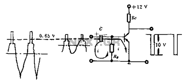
Amplitude separation circuit. A typical amplitude separating circuit is composed of a transistor, capacitance C, and resistances RB and RC. The input signal is a composite video signal, typically with a peak-to-peak voltage of about 2V. The output signal...
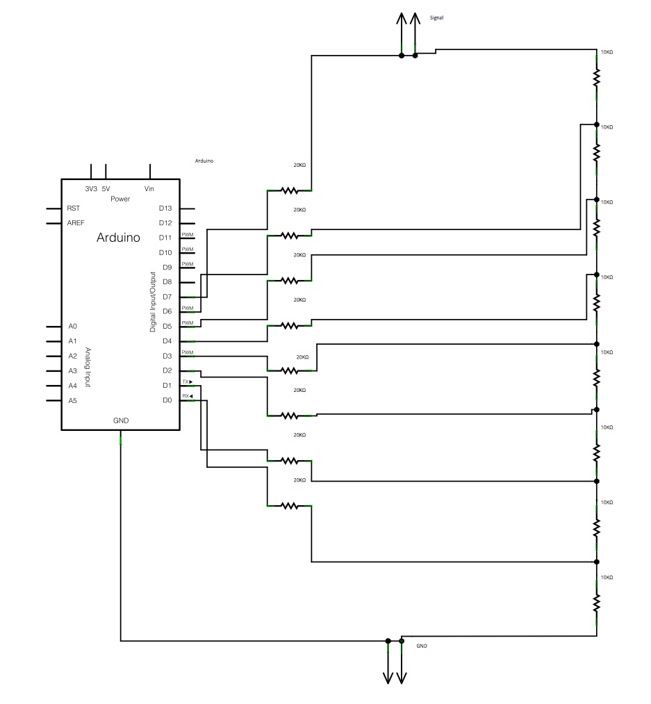
The main concept is to space the time intervals to increment the DAC output values. There are 256 levels since there are 8 digital outputs from the Arduino board. Therefore, for an 8-bit resolution and a 50-second ramp time,...
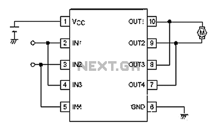
A simple motor control project for forward and backward drive can be implemented using the LB1948M motor driver IC, which features two channels for motor control. The LB1948M is an ideal choice for 12V motor drive systems and can...
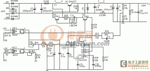
The programmable power supply is a component of an integrated test system for guided missiles, designed to provide and test various required stabilized direct current voltage supplies for guided missiles. It features real-time monitoring, overvoltage protection, and automatic overload...
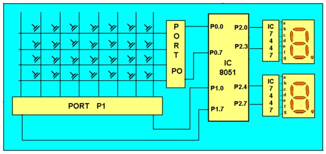
The keyboard being interfaced is a matrix keyboard designed with specific rows and columns. These rows and columns connect to the microcontroller via its ports, specifically the 8051 microcontroller. An 8x8 matrix keyboard is typically used, allowing connection to...
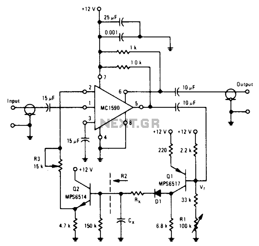
An amplifier designed to achieve a voltage gain of approximately 20, utilizing the MPS6517 PNP transistor in the emitter follower configuration. The RI controller allows for adjustment of the transistor's quiescent point. The output signal is activated only when...