
Speech compression circuit diagram

The amplifier circuit operates by leveraging the characteristics of the MPS6517 PNP transistor in an emitter follower configuration, which provides a high input impedance and low output impedance, making it suitable for driving loads. The voltage gain of approximately 20 indicates that the output voltage is 20 times the input voltage, allowing for significant amplification of weak signals.
The RI controller plays a crucial role in setting the static operating point of the transistor, ensuring optimal performance. By adjusting the quiescent point, the circuit can accommodate varying signal levels and maintain linearity in amplification. The reference voltage Vr, set at 7.0V, serves as a threshold that must be surpassed for the diode D1 to conduct. This feature prevents the amplifier from responding to noise or low-level signals, thus enhancing the signal-to-noise ratio.
When the input signal's peak exceeds the reference voltage Vr, diode D1 becomes forward-biased and conducts, allowing the positive peaks of the signal to pass through. This rectification process is essential for converting the AC signal into a usable DC output. The subsequent filtering stage, which includes capacitor Cx and resistor Rx, smooths the output signal, removing unwanted fluctuations and providing a stable voltage level.
The resistor Rx is particularly important as it determines the charging and discharging time constants for capacitor Cx. A larger resistance value will result in a longer time constant, leading to slower charging and discharging of the capacitor, which can be beneficial for applications requiring a gradual response. Conversely, a smaller resistance value will lead to a quicker response, making the circuit more reactive to changes in the input signal.
In summary, this amplifier circuit effectively manages signal amplification and processing through careful design considerations, including the choice of transistor, the implementation of a quiescent point adjustment mechanism, and the incorporation of rectifying and filtering components. These elements work together to ensure reliable performance in various electronic applications.Amplifier capable of driving a voltage gain of about 20 MPS6517 PNP type emitter electrode group is. RI controller can change the static point of the transistor Q, which is to change the quantity exceeds the signal level Vr. Only when the peak is greater than Vr when (Vr F7.0V), the output of the diode D1 can be rectified positive peaks Q1. The resulting output filters Cx and Rx. Rx control the charging time constant or time out. Charging and discharging are required to use Cx.
Related Circuits
This white LED floodlight illuminates your porch with cool white light. The circuit features a simple and energy-saving design, with a low current consumption. The LED floodlight circuit typically consists of a power supply, a control circuit, and the LED...
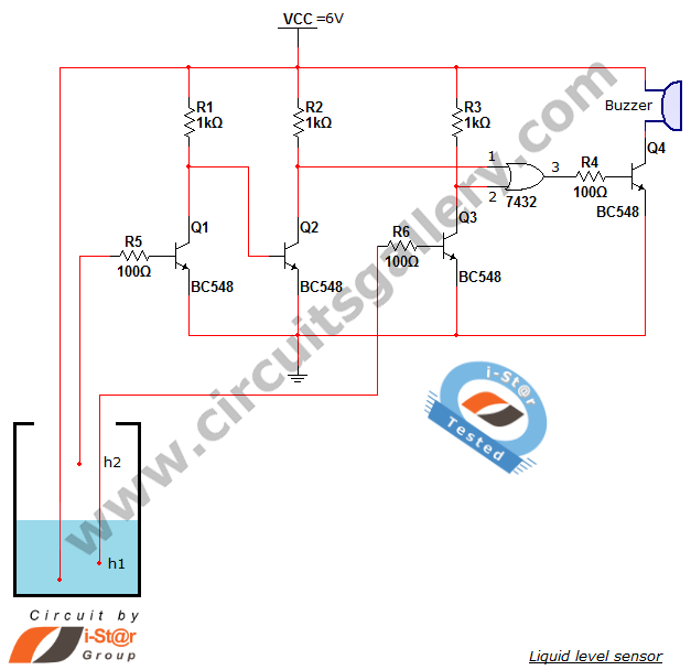
A variety of small electronic projects related to water level sensors have been posted in the Circuits Gallery. This particular project is designed for school students to detect the water level within a water tank or any other water...

This relay driver enhances the input impedance using a standard BC547 NPN transistor (or its equivalent). It is a widely used driver capable of operating various relays, including reed relays. Transistors Q1 and Q2 function as a simple common-emitter...

The following circuit illustrates the circuit diagram of a motor control unit. This circuit is based on the LM317 integrated circuit. Features include diodes that protect the regulator. The motor control unit circuit utilizes the LM317 voltage regulator to provide...
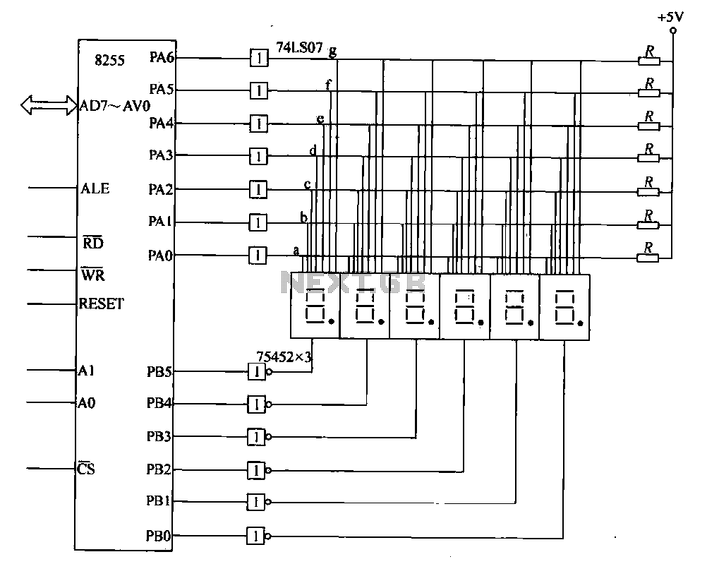
This circuit demonstrates a typical six-digit dynamic display configuration. It utilizes the PA 8255 for display output code and the PB port for bit selection code. The display buffer is designated as DISBUF, which processes the hexadecimal number obtained...
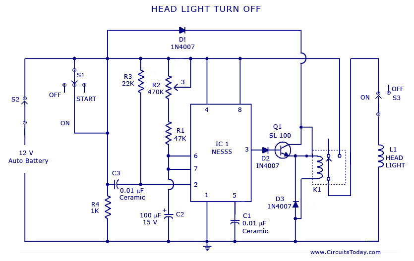
A circuit that can automatically turn off the headlights or lamps of a vehicle after a preset time. This light switching circuit is constructed using a 555 timer integrated circuit (IC). The described circuit utilizes the 555 timer IC in...