
Programmable voltage controlled timer

The µA2240 integrated circuit is designed to function as a versatile programmable timer, leveraging its internal architecture to deliver precise timing functions with minimal component requirements. The key feature of this device is its modulation input, which facilitates external control over the timing characteristics. By connecting a variable voltage from a potentiometer, users can dynamically adjust the input threshold, allowing for flexible timing applications.
The time base output (TBO) is a critical component of the µA2240's functionality. It operates in an open-collector configuration, which allows for easy interfacing with other digital circuits. The inclusion of a 10 kΩ pull-up resistor ensures that the output can be reliably pulled high when not actively driven low by the TBO. This configuration not only enhances signal integrity but also enables the TBO to drive subsequent logic stages, such as the 8-stage counter, effectively expanding the timer's capabilities.
Upon receiving a positive trigger pulse at startup, the TBO initiates its timing cycle, resetting all counter outputs to a low state. The open-collector nature of the counter outputs allows for a "wired-OR" logic configuration, where multiple outputs can be combined to generate a single output signal. This feature is particularly useful in applications requiring multiple timing conditions to be monitored simultaneously.
The µA2240's architecture supports the generation of up to 255 discrete time delays, each corresponding to integer multiples of the time-base period. This is accomplished by summing the binary outputs of the counter, providing a flexible method for achieving various timing requirements. The range of delays, from 200 µs to 0.223 s, makes the µA2240 suitable for a wide range of timing applications in both consumer and industrial electronics. Overall, the µA2240 presents a robust solution for programmable timing needs, combining ease of use with extensive functionality.The µA2240 may easily be configured as a programmable voltage controlled timer with a minimum number of external components. The modulation input (pin 12), which allows external adjustment of the input threshold level. A variable voltage is applied from the arm of a 10 k ohm potentiometer connected from Vcc to ground. A change in the modulation input voltage will result in a change in the time base oscillator frequency and the period of the time base output (TBO).
The TBO has an open-collector output that is connected to the regulator output via a 10 k ohm pull-up resistor. The output of the TBO drives the input to the 8-stage counter section. At start-up, a positive trigger pulse starts the TBO and sets all counter outputs to a low state. The binary outputs are open-collector stages that may be connected together to the 10 k ohm pull-up resistor to provide a "wired-OR" output function. This circuit may be used to generate 255 discrete time delays that are integer multiples of the time-base period.
The total delay is the sum of the number of time-base periods, which is the binary sum of the Q outputs connected. Delays from 200 µß to 0.223 s are possible with this configuration.
Related Circuits
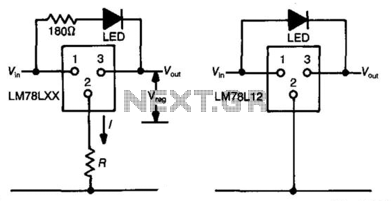
The three-terminal regulator device (LM78LXX) provides an output voltage (Vout) equal to the input voltage (Vm) until the input voltage exceeds the output voltage by 1.5 to 2 volts. A regulated voltage (Vreg) is achieved at this point, with...
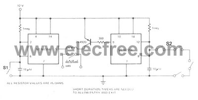
The car burglar alarm timer system circuit is designed to be economical and convenient for installation in an automobile. Typically, a switch is set up to connect with the automobile door, which keeps the circuit closed. However, if the...
This circuit charges two NiCad cells with a constant current and features dual charging rates, voltage cutoff, and an audible alarm. The circuit is powered. This circuit is designed to efficiently charge two nickel-cadmium (NiCad) cells, utilizing a constant current...
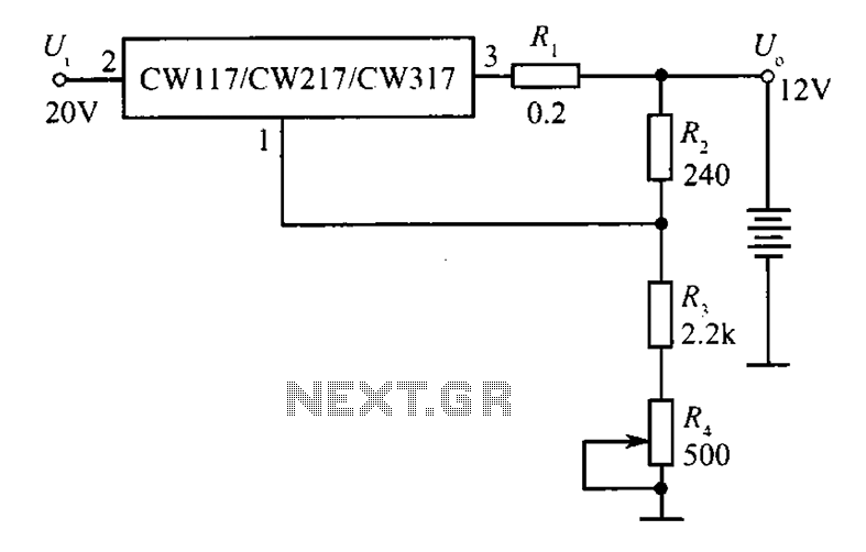
A 12V constant voltage charger is depicted. The power supply circuit shares the same basic design. The resistor R1, valued at 0.2 ohms, serves a limiting function, effectively increasing the internal resistance of the charger, which in turn reduces...
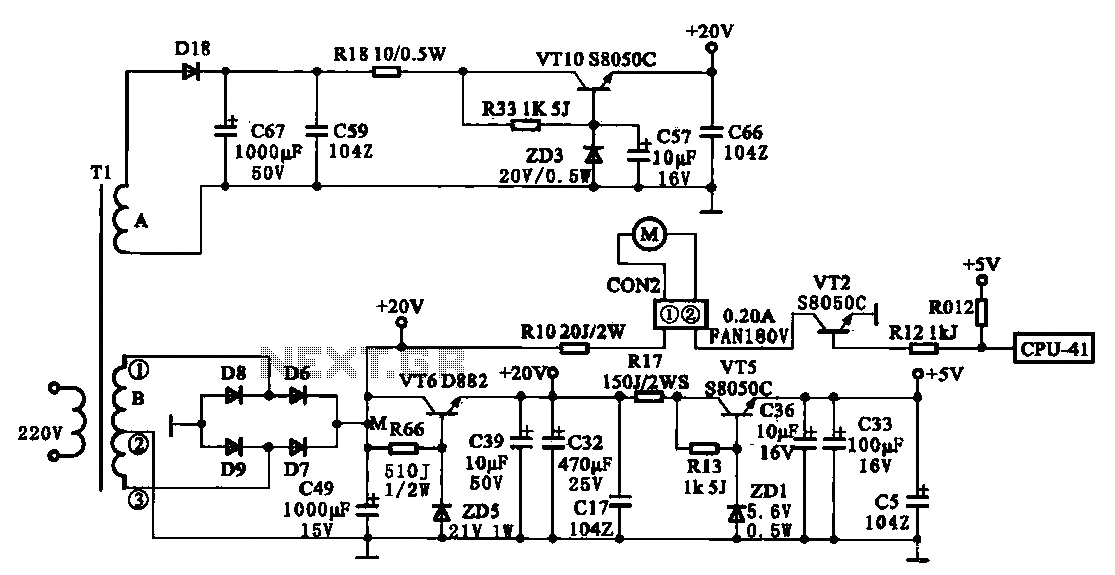
The JYC-22F type cooker low voltage power supply circuit is depicted. An AC 220 V power supply voltage is applied to a low-voltage transformer. The transformer has a primary winding (Tl) and two secondary windings (A and B), with...

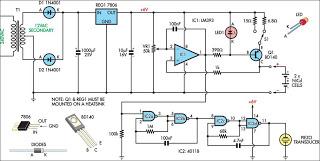
This timer was designed primarily to turn off a portable radio after a specific duration. This feature allows users to fall asleep on the beach or in a hammock, with the assurance that the radio will automatically shut off...