
Pulse-width modulator

In a monostable timer circuit, such as those utilizing the 555 timer IC, the operation relies on a single stable state and a temporary unstable state. When triggered by a pulse, the timer generates a single output pulse of a defined duration. The width of this output pulse is primarily determined by the time constant formed by the resistor-capacitor (RC) network connected to the timing capacitor.
In this configuration, pin 3 serves as the control voltage input, allowing for dynamic adjustment of the threshold voltage that dictates when the timer resets. By varying the voltage at pin 3, the effective threshold voltage can be modified, thus altering the charge time of the capacitor. This adjustment leads to a change in the output pulse width, enabling applications such as pulse width modulation (PWM) where precise control over the pulse duration is required.
The ability to apply a modulating signal to pin 3 introduces an additional layer of flexibility. This signal can be derived from various sources, such as a potentiometer, another waveform generator, or a digital control signal, allowing for real-time modulation of the output pulse width. This feature is particularly useful in applications where the timing characteristics need to adapt to varying conditions, such as in motor speed control, light dimming, or audio signal processing.
The overall functionality of the monostable timer in this context emphasizes the importance of the RC network and control voltage manipulation, showcasing its versatility in electronic design for a range of applications requiring precise timing control.if the timer is triggered with a continuous pulse train in the monostable mode of operation, the charge time of the capacitor can be varied by changing the control voltage at pin 3 In this manner, the output pulse width can be modulated by applying a modulating signal that controls the threshold voltage.
Related Circuits
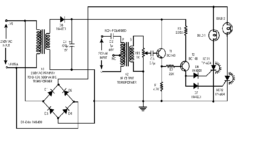
Audio light modulations add to the enjoyment of music during functions organised at home or outdoors. Presented here is one such simple circuit in which light is modulated using a small fraction of the audio output from the speaker...
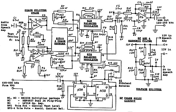
The circuit details are presented in Figure 3. The primary components of the system include a speech amplifier, an audio phase shift network with a balanced driver circuit (N1A, N2A), two balanced modulator stages (N1B & N2B), an RF...
The TLE6282G is an H-Bridge and Half Bridge Driver IC designed for high-current DC brush motor applications in PWM control mode. It is suitable for use in injector and valve applications across 12V, 24V, and 42V power networks. This...
More: An electronic schematic is a representation of the components and connections within an electronic circuit. It serves as a blueprint for constructing electronic devices, allowing engineers and technicians to visualize how components interact and function together. The schematic...

Provides at least 200 kHz deviation when applied to the base of the oscillator transistor, before severe distortion sets in. Feedback keeps output impedance low. -D. Enemark, Transistors Improve Telemeter Transmitter, Electronics, 32:11, p 136-137. The described circuit operates by...
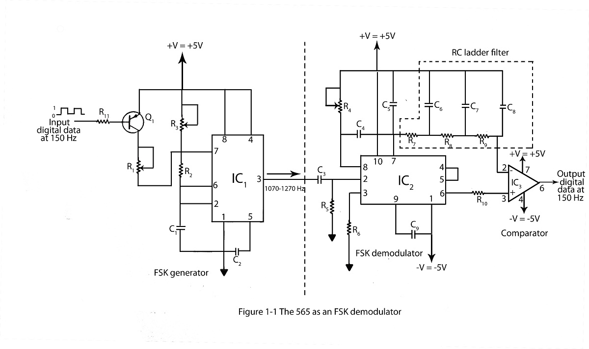
The frequency shifting keying technique is utilized to transmit binary data. The circuit diagram includes a description of an FSK demodulator that employs the 565 integrated circuit for frequency shift keying. The frequency shift keying (FSK) technique is a form...