
PWM Motor/Light Controller

The described circuit consists of two distinct configurations intended for PWM (Pulse Width Modulation) control, specifically designed for 12V applications. The configurations include a low-side switching arrangement utilizing an N-channel MOSFET and a high-side switching arrangement utilizing a P-channel MOSFET.
In the low-side configuration, the N-channel MOSFET is connected between the load and ground. This arrangement allows for efficient current handling due to the inherent characteristics of N-channel devices, which typically offer lower on-resistance and higher current capacity compared to P-channel devices. The IRFZ34N MOSFET, capable of handling over 35 Amps, is recommended for this configuration, especially when paired with an adequate heat sink to manage thermal performance. For applications requiring even higher current capabilities, alternative MOSFETs such as the IRFZ48N or IRF1010Z may be utilized.
Conversely, the high-side configuration connects the P-channel MOSFET between the power supply (12V) and the load. This setup is particularly beneficial when it is necessary to ground one side of the load, which is a common requirement in various applications. Although P-channel devices are generally more expensive and less efficient in terms of current handling, they serve a critical role in circuits where high-side switching is essential.
Both configurations are designed to operate under PWM control, allowing for efficient modulation of power delivered to the load. The choice between high-side and low-side configurations depends on the specific requirements of the application, including load characteristics and the necessity of grounding one side of the load. Proper selection and implementation of the MOSFETs, along with appropriate thermal management, are crucial for ensuring reliable operation of these PWM circuits.These two schematics are variations on another PWM circuit that I designed. The diagrams are for 12V operation only and there are high side (common ground) and low side (common +12V) versions. The low side version of the circuit uses an N Channel FET, the high side version of the circuit uses a P Channel FET.
N Channel devices tend to handle more current than P Channel devices, they are also less expensive. The high side version of the circuit is useful when one side of the load has to be grounded. This circuit can switch a fairly high amount of current, an IRFZ34N MOSFET can handle over 35 Amps if connected to a proper heat sink. Higher power FETs, such as the IRFZ48N or IRF1010Z can be substituted if even larger currents are required.
It is also p 🔗 External reference
Related Circuits
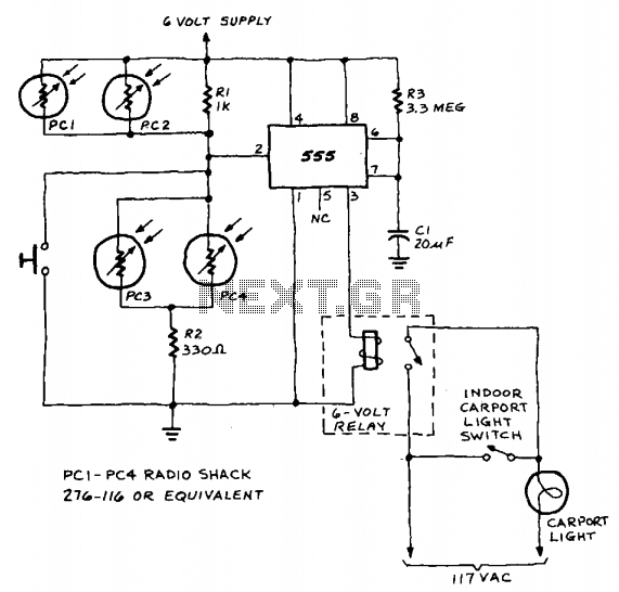
A 555 timer integrated circuit (IC) functions in one-shot mode, triggered by light exposure to photoresistors. These photoresistors typically exhibit a resistance in the range of several megohms, which decreases to several hundred ohms under light conditions, allowing current...
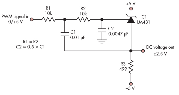
This simple circuit converts a 5V PWM signal into a variable precision reference voltage with a range of -2.5V to +2.5V. Many designs, such as a digitally controlled power supply or a programmable dummy load, require a Digital to...
There are two types of solar automatic tracking controllers. One type utilizes a Schmitt trigger light control, which consists of a light sensor and a Schmitt trigger or monostable trigger. The second type employs two light sensors and two...

A neon bulb and a CdS photocell are enclosed in a light-tight enclosure to form an optocoupler. A diac/triac combination is employed to create a snap-switch effect. A second CdS photocell serves as the primary sensor. As darkness approaches,...
The primary objective is to present the circuit diagram and describe the software utilized. A UDP application is employed to transmit commands to the microcontroller, which subsequently activates or deactivates the relay. It is anticipated that TCP implementation could...
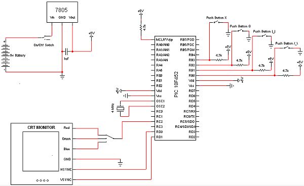
The objective of this project is to develop a device capable of outputting VGA signals to a CRT monitor to display figures, text, and characters. The project involves designing a circuit that generates standard VGA signals, which include separate horizontal...