
Quiz game schematic

The jam circuit described is designed to facilitate a competitive quiz environment by allowing up to eight contestants to signal their readiness to answer questions. Each contestant is assigned a unique number from 1 to 8, which is represented on a display when they press their respective button (switch). The circuit utilizes the 74LS373 transparent latch (IC1) to capture the state of the switches when pressed. Upon pressing the reset switch S9, all outputs of IC1 are set high, allowing the circuit to initialize in a known state.
The outputs from IC1 are connected to the inputs of a priority encoder (74LS147, IC2) and an 8-input NAND gate (74LS30, IC3). The NAND gate's output transitions to a logic 0 state, which is then inverted by NAND gate N2 to control the latch-enable pin of IC1. This ensures that when a contestant presses their switch, the corresponding output of IC1 is latched low, indicating their selection on the display.
The 7-segment display is driven by the 74LS47 decoder/driver (IC6), which receives a BCD output from IC2. The display shows a zero initially, and when a switch is pressed, the display updates to reflect the contestant's number. The circuit includes logic that prevents any subsequent switch presses from altering the displayed number once a contestant has signaled first, effectively "jamming" the display to show the first contestant's number.
In scenarios where two switches are pressed almost simultaneously, the priority encoder ensures that the contestant with the lower assigned number is displayed, thus maintaining a fair competitive environment. The buzzer, which indicates the activation of the circuit, is controlled by a PNP transistor (BC158, T1), activated by the output of NAND gate N1 when a switch is pressed. The reset functionality allows for the system to be cleared quickly, preparing it for the next round of competition. This circuit design incorporates essential digital logic components to achieve its intended functionality, providing an effective solution for quiz contests.This jam circuit can be used in quiz contests wherein any par- ticipant who presses his button (switch) before the other contestants, gets the first chance to answer a question. The circuit given here permits up to eight contestants with each one allotted a distinct number (1 to 8).
The display will show the number of the contestant pressing his button before the others. Simultaneously, a buzzer will also sound. Both, the display as well as the buzzer have to be reset manually using a common reset switch. Initially, when reset switch S9 is momentarily pressed and released, all outputs of 74LS373 (IC1) transparent latch go high since all the input data lines are returned to Vcc via resistors R1 through R8. All eight outputs of IC1 are connected to inputs of priority encoder 74LS147 (IC2) as well as 8-input NAND gate 74LS30 (IC3). The output of IC3 thus becomes logic 0 which, after inversion by NAND gate N2, is applied to latch-enable pin 11 of IC1.
With all input pins of IC2 being logic 1, its BCD output is 0000, which is applied to 7-segment decoder/driver 74LS47 (IC6) after inversion by hex inverter gates inside 74LS04 (IC5). Thus, on reset the display shows 0. When any one of the push-to-on switches S1 through S8 is pressed, the corresponding output line of IC1 is latched at logic 0 level and the display indicates the number associated with the specific switch.
At the same time, output pin 8 of IC3 becomes high, which causes outputs of both gates N1 and N2 to go to logic 0 state. Logic 0 output of gate N2 inhibits IC1, and thus pressing of any other switch S1 through S8 has no effect.
Thus, the contestant who presses his switch first, jams the display to show only his number. In the unlikely event of simultaneous pressing (within few nano-seconds difference) of more than one switch, the higher priority number (switch no.) will be displayed. Simultaneously, the logic 0 output of gate N1 drives the buzzer via pnp transistor BC158 (T1). The buzzer as well the display can be reset (to show 0) by momentary pressing of reset switch S9 so that next round may start.
Lab Note: The original circuit sent by the author has been modified as it did not jam the display, and a higher number switch (higher priority), even when pressed later, was able to change the displayed number. 🔗 External reference
Related Circuits

Schematic for the SPI Supplies Faraday Cup. This document provides a detailed examination of the diagrams for the SPI Supplies stand-alone Faraday Cup, which is utilized for calibrating beam currents in wavelength dispersive electron microprobes, as well as interfacing...
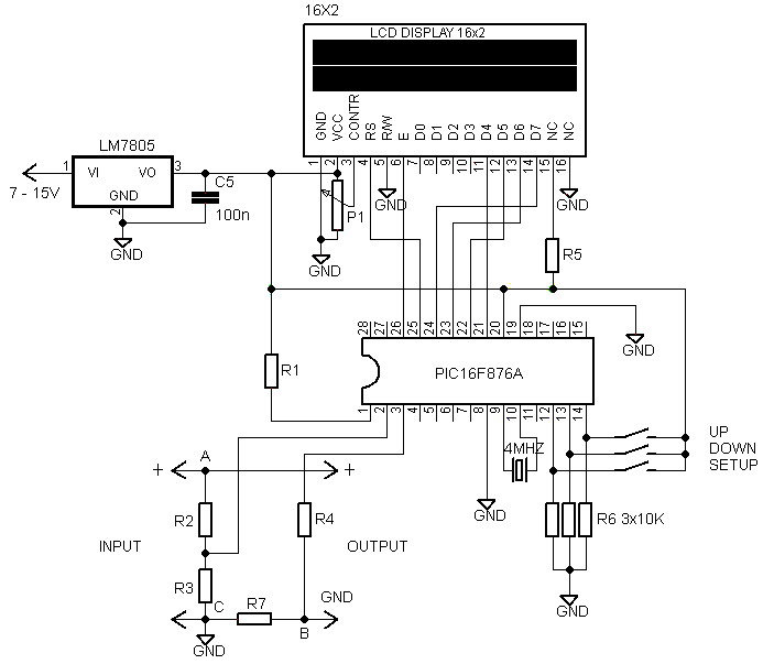
Voltmeters and ammeters with a PIC microcontroller can be utilized to measure voltage and current simultaneously. The configuration of voltmeters and ammeters using the PIC16F876A serves as a data processor for voltage and current measurements. This circuit employs a...
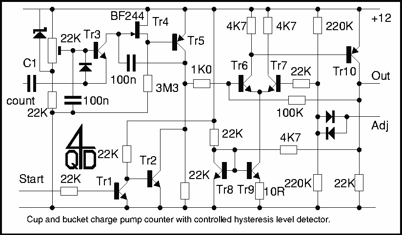
It was designed for an application in a welding machine: there are lots of bits of machinery which are cylindrical in shape and which are subjected to heavy surface wear. For instance ore crushers, and the idler and roller...
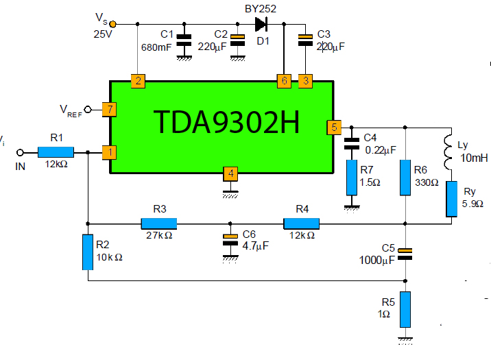
The TDA9302H is a monolithic integrated circuit housed in a HEPTAWATTTM package. It functions as a high-efficiency power amplifier designed for direct drive vertical deflection coils in television yokes. This component is suitable for use in both color and...
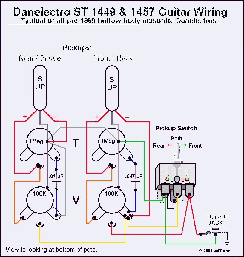
Using a magnetic compass, ensure that both pickups have a South polarity on the top of each pickup. Verify this by checking for a North polarity on the bottom of the pickups. It is uncommon to find both pickups...

Martin Ustek has modified the project to include a Sokoban game. Information about his version can be found throughout this page; for full details, please visit his website (Czech). Either game can be selected with a menu that appears...