
radio controlled toy car

The transmitter schematic also includes NOR gate U2A, which forms a latch circuit (U2C, RS Flip Flop). The influence of resistor R2 and capacitor C11 feeds into pin 9 on U2C. When the electrical circuit activates U2C, the output becomes high (`1`), causing U2A output (pin 3) to drop to low (`0`). This condition triggers the clock generator U2B to operate, while simultaneously resetting the counter IC (U1, 14024), allowing U1 to begin chopping the 27.145 MHz oscillator circuit to produce a working clock frequency.
The second part of the circuit is the receiver, which is paired with the toy car. It receives signals from the transmitter to control the car's movements (forward, backward, left, right). Transistor Q1, along with resistors and capacitors, forms a radio signal receiver circuit for 27.145 MHz. T1 in this configuration is identical to the one used in the transmitter circuit. The receiver schematic includes transistor Q2, which converts the received radio frequency pulses into a pulse format acceptable as a digital signal by the CMOS IC. This digital signal serves as a clock for the counter IC (U2, 14024). The output from IC 14024 corresponds to the number of pulses sent by the transmitter, with specific pulse counts representing commands for forward and left movements (for example, 24 pulses). The output from 14024 generates signals Q4 = `1`, Q5 = `1`, Q6 = `0`, and Q7 = `0`.
The first control pulse appears after the transmission stops, with the pulse frequency interval between code deliveries being crucial. This pulse is used to record the results in U3 (14042, a D Flip Flop) from 14024, ensuring that the final state of 14024 retains control over the motor. Following the recording, 14042 counts double with the second pulse, allowing for a reset of 14042 after a lag time.
The circuit is further enhanced by transistors Q3, Q4, Q7, Q8, Q9, and Q10, which form an H-bridge circuit, a reliable configuration for driving DC motors. This arrangement allows for directional control of the DC motor, enabling it to rotate either left or right, or to stop. The operation of this circuit requires opposing base voltages for Q7 and Q10; for instance, if Q7 is high (`1`) and Q10 is low (`0`), the motor will rotate left, while the opposite configuration will cause it to rotate right. If both are low (`0`), the motor will stop. It is critical to avoid a scenario where both Q7 and Q10 are high (`1`). Similarly, transistors Q5, Q6, Q11, Q12, Q13, and Q14 also form an H-bridge configuration. The left H-bridge controls the motor for lateral movements, while the right H-bridge manages forward and backward motions. The relationship between 14042 and the counting input/output of D Flip Flop 14024 is designed to ensure that feedback signals to each H-bridge cannot all be high (`1`) simultaneously.This circuit is a circuit diagram of the radio-controlled, usually in the toy car application children. Circuit diagram consists of 2 parts of the circuit sender and receiver circuits. To the circuit sending radio signals generated by the oscillator circuit formed by transistors Q1 9016, operating frequency of the oscillator is determined by the c
rystal Y1 is worth 27. 145 MHz. A very critical part of this oscillator circuit is T1, L1 and L2, which specifically discussed separately at the end of this article. Working from this oscillator is controlled by NOR gate U2D 14001, when the output gate (pin 3) value of `1, the oscillator will work and send radio frequency 27.
145 MHz, and the output U2D value `0 ² the oscillator will stop working. U2D NOR gate receives the clock signal from NOR gate U2B. CMOS NOR gate with the help of resistors R4 and R5 and capacitor C8 form a low frequency shaping circuit for controlling clock oscillator existing digital circuits. Work from clock generator is controlled through the input leg 6, the circuit will increase if the input clock level `0.
Here is a circuit schematic drawing transmitter: NOR gate U2A and form a latch circuit U2C (RS Flip Flop), because the influence of R2 and the capacitor C11 is fed to pin 9 on U2C, when an electrical circuit to U2C output `1 and U2A output (pin 3) becomes `0. This situation resulted in generating the generator akang U2B hours working hours and state of the counter reset 14024th IC (U1), so that U1 started chopping and 27.
145 MHz oscillator circuit sending pulses to produce a working clock frequency. Part two is the receiver. Receiver circuit which in pairs in a toy car, works receive signals from the transmitter to control the motor car, so the car can move forward / backward and left / right. Transistor Q1 with the help of resistors, capacitors and T1 form as a series of radio signal receiver 27.
145 MHz. T1 in this series exactly the same as those used in the transmitter circuit T1. Here is a circuit schematic drawing receiver: The following equipment transistor Q2 to form a series of changes in the radio frequency pulses are received from the transmitter into the box pulses that can be accepted as a digital signal by the CMOS IC. This digital signal will be accepted as a clock that will be chopped by 14, 024 to calculate IC (U2).
The output will be 14024 according to the number of pulses sent by the transmitter, forward orders and left (which is used for example in the discussion of the transmitter) is a pulse of 24, the pulse count output from 14024 to produce Q4 = `1, Q5 = `1 ², Q6 = `0 and Q7 = `0 ². The first control pulse will appear after it stopped sending because the pulse frequency interval between the delivery of code, this pulse serves to record the results of U3 14042 minced 14024 (D Flip Flop), so that the final conditions for the 14024 retained control of the motor.
After the results recorded 14042 to 14024, 14042 double-counting by the second pulse, so that after passing the lag time can be cut from 14042 to calculate 0 again. Circuit formed by transistors Q3, Q4, Q7, Q8, Q9 and Q10-called H bridge circuit, this circuit is very reliable to drive DC motors.
With this series of DC motor can be rotated to the right, left or stop motion. The main requirement is the use of this circuit the base voltage Q7 and Q10 base voltage must be opposed, for example, the base Q7 = `1 and the base of Q10 = `0 ² the motor rotates to the left, the base Q7 = `0 and the base of Q10 = `1 ² the motor will turning to the right, the base Q7 = `0 and the base of Q10 = `0 ² the motor to stop motion, but it should not happen the base Q7 = `1 and the base of Q10 = `1 ². Similarly, Q5, Q6, Q11, Q12, Q13 and Q14 form an H Bridge. H Bridge on the left side of Figure 2 is used to control a motor that regulates the motion of cars left / right, while the right side of the H bridge is used to control a motor that regulates movement forward / backward a car.
Relations between 14, 042 and counting input output D Flip Flop was 14024th constructed so that the feedback signals to each H bridge can not be all `1 simultaneously. 🔗 External reference
Related Circuits
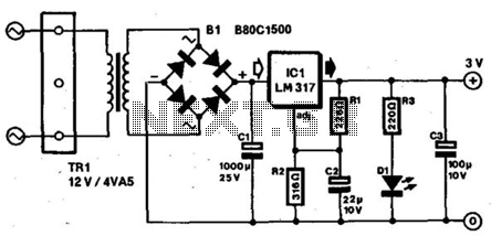
Most small portable radios require a 3-V supply, which is typically provided by two AA or AAA batteries. Many of these radios are equipped with a charger socket since rechargeable batteries are an option. When used in a stationary...

The LR inputs are summed, processed, and then drive a comparator. This comparator detects levels and generates transitions when audio inputs exceed or fall below predetermined thresholds. The frequency of these transitions, which correspond to rapid volume changes, is...
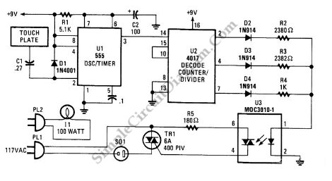
This is a three-mode lamp dimmer circuit with touch control. This circuit can be used to control a lamp in three operation modes: dim, off, and bright. A NE555 timer is utilized in the design. The three-mode lamp dimmer circuit...
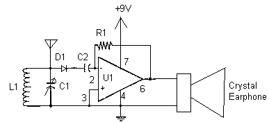
Here is a simple radio that is easy to build and inexpensive. In fact, you probably have all the parts you need in your junk box. You'll be surprised at the great reception with this little set. More: The...

User Agreement & Disclaimer Disclaimer: All files are found using legitimate search engine techniques. This site does not condone hacking into sites to create the links it lists. It is assumed that all links found on the search...
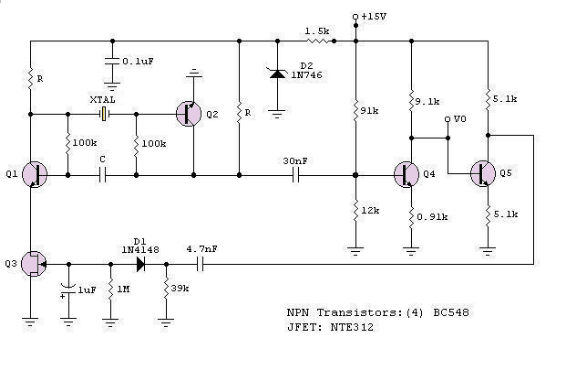
The RF engineer often needs an instrument that can reliably and quickly test a low-frequency quartz crystal unit. However, such equipment is challenging to find, and engineers frequently consult electronic circuit handbooks for schematics that can accomplish this task....