
Rear Fog Light Controller With Delay

The rear fog light delay circuit is designed to enhance road safety by preventing abrupt reactions from following drivers. The circuit operates through a combination of a MOSFET and passive components, which control the gradual illumination of the fog lights. The switch S1 acts as the primary control element, allowing the driver to activate the fog lights when needed.
Upon activation, the MOSFET T1 begins to conduct, and the gate-source voltage (Vgs) is crucial for controlling the rate at which the lights brighten. The time constant, determined by the resistor R2 and capacitor C1, plays a significant role in establishing the delay period. This delay allows the driver to switch on the fog lights without immediately blinding the drivers behind, which could lead to confusion or accidents.
The preset PI is an essential feature of the circuit, as it provides initial bias to the MOSFET, ensuring that the fog lights can illuminate weakly before achieving full brightness. This design consideration enhances the circuit's effectiveness by allowing for a smoother transition in light intensity, thereby minimizing the risk of misinterpretation by following vehicles.
In terms of thermal management, the dissipative characteristics of the MOSFET T1 during the transitional phase must be carefully evaluated. The heatsink should be designed based on the maximum dissipation during full lamp operation, ensuring that the component remains within safe operating temperatures even under prolonged use.
Overall, this rear fog light delay circuit not only improves visibility in adverse weather conditions but also contributes significantly to overall traffic safety by mitigating the risk of sudden braking reactions from trailing vehicles. We assume that most of our readers are thoughtful drivers who do not switch on their rear fog lights w hen closely followed by other traffic. Following drivers (for an instant) will think that you are braking (although they have seen no reason for your doing so) and thus slam on their brakes as well. This could cause a very dangerous situation. Avoid a potentially dangerous action and install the rear fog light delay circuit, presented here. Switch Si is the on/off control for rear fog lights LI and L2. As soon as this switch is closed, the gate-source voltage (Vgs) of MOSFET T1 will become more and more negative.
Thus, the IC will conduct harder and harder. This in turn causes the brightness of the lights to gradually become brighter. Maximum brightness is reached after a delay of about 20 seconds, which is determined by time constant R2/C1. The gate of T1 can be given a bias by preset PI. This provides compensation for the initial period after the lights are switched on and the lamps do not light, because they need hundreds of milliamperes before they can do so.
With PI set correctly, the lamps will light, albeit weakly, and immediately the control switch is closed. The gate potential is then equal to the voltage at the wiper of PI (remember that CI is then still discharged).
Although the dissipation of T1 is a maximum during the transitional period (between switch on and the lamps lighting brightly), the heatsink required is calculated on the basis of the dissipation when the lamps light brightly.
Related Circuits
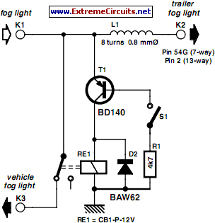
In many countries, it is now mandatory or at least recommended to have a rear fog light on a trailer. There is an additional requirement that when the trailer is connected to the vehicle, the rear fog light of...
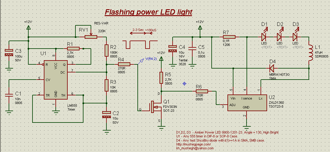
This project demonstrates the construction of a simple flashing light circuit using the IC 555 timer. The 555 timer functions as a clock generator with a duty cycle of less than 100% and greater than 50%. Additional components include...
A wooden table features numerous holes of varying diameters designed to accommodate optical fibers. Due to the size of the ceiling lamp (90 cm x 60 cm), it was not feasible to utilize a single bundle of fibers, resulting...

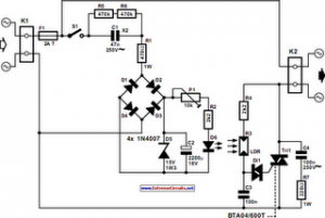
The circuit presented here ensures that if bulb La1 fails, bulb La2 will take over its function. In series with La1 is triac Tri2. Resistor R3 and capacitor C2 form a delay network. When the voltage across C2 exceeds...
The following circuit illustrates an Automatic Light Dimmer Circuit Diagram utilizing a 1N4007 diode. Features include integration within a wall-mounted box. The Automatic Light Dimmer Circuit is designed to adjust the brightness of a light source automatically based on ambient...
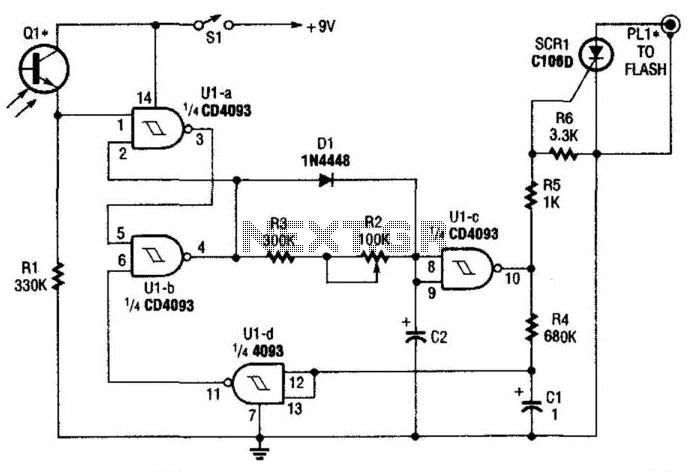
Q1 is a phototransistor that is normally illuminated by a beam of light. When the beam is interrupted, pin 1 of U1A goes high, which forces pin 4 of U2B low. Consequently, capacitor C2 discharges through resistors R2 and...