
Receiver for 50 khz optical transmitter

The described receiver circuit is engineered to optimize performance in environments where signal integrity is paramount. The L14G2 detector serves as the initial signal processing element, converting incoming optical signals into electrical currents. This is followed by two gain stages that amplify the signal while maintaining a careful balance to preserve the signal-to-noise ratio. The FM demodulator, adapted from a tachometer design, processes the amplified signal to recover the frequency-modulated information, allowing for accurate measurement and interpretation of the received data.
Incorporating additional stages of stabilized gain with AGC can enhance the sensitivity of the receiver. AGC automatically adjusts the gain of the amplifier stages based on the incoming signal strength, ensuring optimal performance across varying signal conditions. This feature is particularly beneficial in applications where signal levels fluctuate significantly.
Alternatively, for applications where cost is a critical factor, the use of an H23A1 emitter-detector pair can simplify the design while still providing adequate performance. This approach may involve the elimination of one or more amplifier stages, which can lead to a more compact and cost-effective solution, albeit at the expense of some sensitivity.
Furthermore, in scenarios where the output voltage is susceptible to noise or interference, additional filtering may be required. This can be accomplished through the implementation of low-pass filters or other filtering techniques that help to smooth out the output signal, ensuring that the final output is clean and representative of the intended measurement.
Overall, the design of this receiver circuit must carefully consider these various factors to achieve a reliable and efficient performance suitable for its intended application.For maximum range, the receiver must be designed in the same manner as a radio receiver front end, since the received signals will be similar in both frequency component and in amplitude of the photodiode current. The major constraint on the receiver performance is signal to noise ratio, followed by e.m. shielding, stability, bias points, parts layout, etc. These become significant details in the final design. This receiver circuit consists of a L14G2 detector, two stages of gain, and a FM demodulator which is the tachometer circuit, modified to operate up to 100 kHz.
Better sensitivity can be obtained using more stages of stabilized gain with AGC, lower cost and sensitivity may be obtained by using an H23A1 emitter-detector pair and/or by eliminating amplifier stages. For some applications, additional filtering of the output voltage may be desired.
Related Circuits
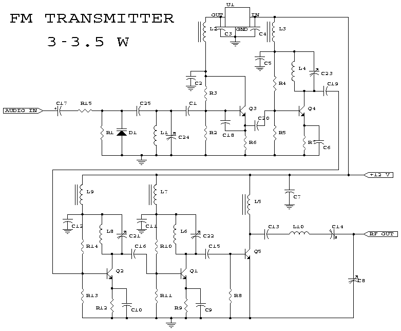
This schematic represents an FM transmitter capable of delivering an output power of 3 to 3.5 watts, operational within a frequency range of 90 to 110 MHz. While the inherent stability of the circuit is acceptable, the implementation of...
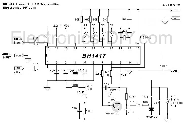
This is the latest BH1417 FM Transmitter design from RHOM that includes a lot of features in one small package. It comes with pre-emphasis, limiter so that the music can be transmitted at the same audio level, stereo encoder...
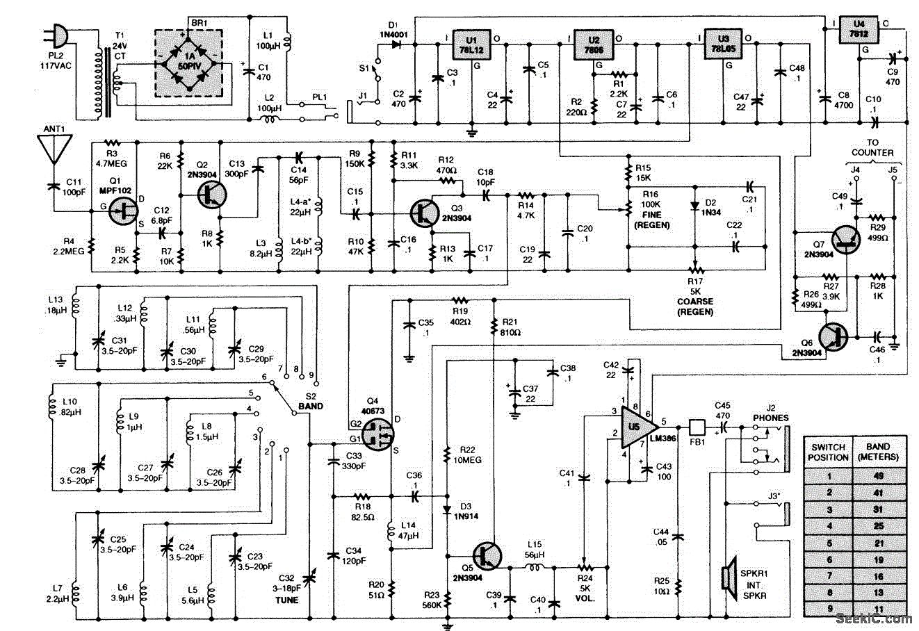
The receiver consists of multiple subassemblies, including an active antenna, an amplifier featuring regeneration control and band-switching circuitry, an AM detector, a power amplifier, and an output device such as an internal speaker, external speaker, or headphones. Additionally, it...
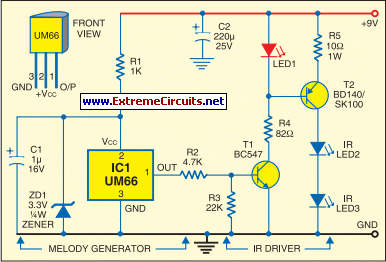
This circuit is designed to generate audio musical notes that can be heard from a distance of up to 10 meters. It consists of two main components: an infrared (IR) music transmitter and an IR music receiver. The IR...
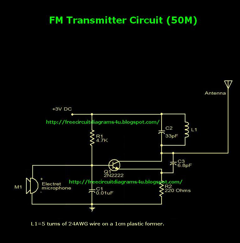
This is an FM transmitter circuit diagram. This circuit uses a 2N2222 transistor, allowing it to operate at 3V and transmit signals up to 50 meters. The FM transmitter circuit consists of several key components, primarily centered around the 2N2222...
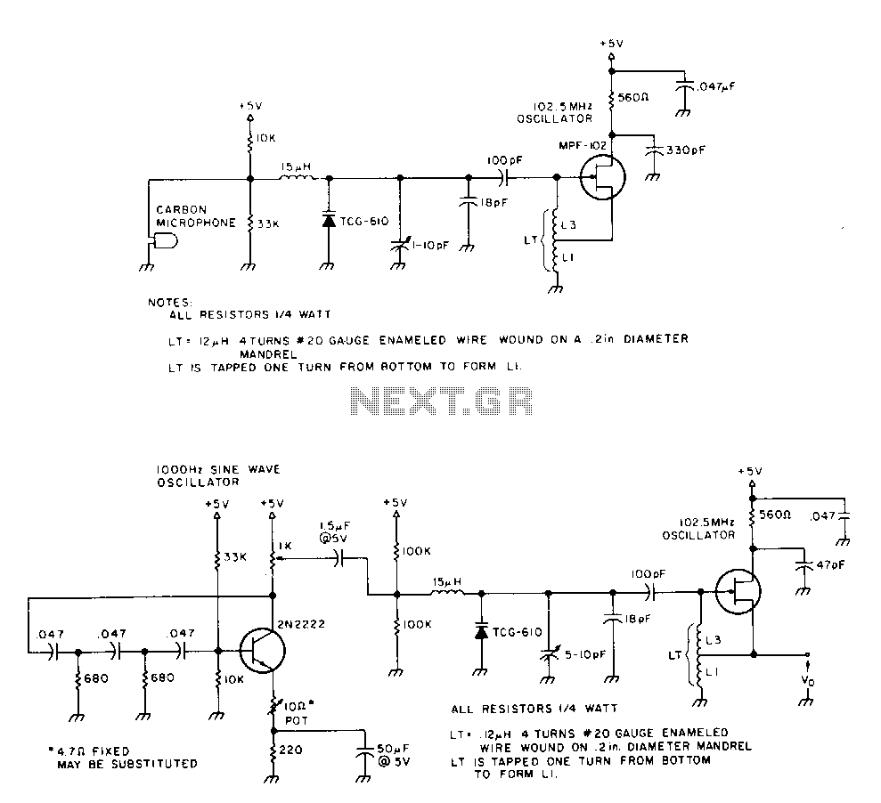
The 2N2222 circuitry is a three-element, phase-shift oscillator circuit designed to produce a 1,000 Hz sine wave. This sine wave is applied to the TCG-610 varactor diode, which has a capacitance of 6 pF at 4 V. This application...