
3W FM Transmitter

This FM transmitter circuit is designed to operate efficiently within the specified frequency range, making it suitable for various applications such as amateur radio broadcasting or personal use. The output power of 3 to 3.5 watts is adequate for local transmission, while the potential for increased power via the BLY88 amplifier allows for expanded reach and versatility.
The circuit's architecture typically includes essential components such as oscillators, modulators, and amplifiers, which work together to generate and transmit the modulated signal. The inclusion of a PLL can significantly improve frequency stability, reducing drift and ensuring consistent performance over time. This can be particularly beneficial in environments where signal integrity is paramount.
Attention to detail during construction is crucial. The use of an RF-proof casing minimizes interference and signal degradation, while high-quality connectors and cables maintain the integrity of the signal path. Proper shielding between stages helps prevent unwanted interactions and noise, which can adversely affect performance. Following RF design principles, such as maintaining appropriate impedance levels and ensuring good grounding practices, is essential for achieving optimal results.
Testing the circuit on an RF breadboard allows for initial validation of functionality, but further testing in a controlled environment is recommended to ensure compliance with local regulations and performance expectations. Overall, this FM transmitter design offers a solid foundation for anyone looking to explore or expand their capabilities in RF transmission.This is the schematic for an FM transmitter with 3 to 3. 5 W output power that can be used between 90 and 110 MHz. Although the stability isn`t so bad, a PLL can be used on this circuit. This is a circuit that I`ve build a few years ago for a friend, who used it in combination with the BLY88 amplifier to obtain 20 W output power. From the notes tha t I made at the original schematic, it worked fine with a SWR of 1 : 1. 05 (quite normal at my place with my antenna). 2. The circuit has been tested on a normal RF-testing breadboard (with one side copper). Make some connections between the two sides. Build the transmitter in a RF-proof casing, use good connectors and cable, make a shielding between the different stages, and be aware of all the other RF rules of building. 🔗 External reference
Related Circuits
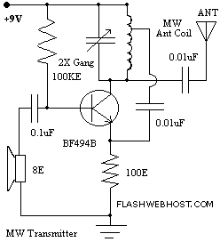
Here is a very simple, inexpensive and interesting project which provides lot of fun to a home experimenter or hobbyist. This simple transmitter can transmit speeches or songs within a short range. The circuit uses only one transistor. The...
The car MP3 FM transmitter circuit is designed to broadcast audio signals to FM receivers. It incorporates a high-quality preamplifier circuit, ensuring that the sound quality of the broadcast is excellent. The car MP3 FM transmitter circuit typically consists of...
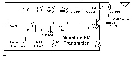
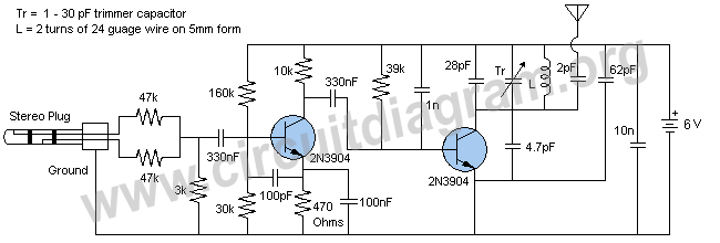
Construct a simple mini FM transmitter. This engaging project demonstrates how to create a mini broadcasting transmitter capable of transmitting an audio signal up to a quarter mile to any FM receiver. It is straightforward to assemble and offers...
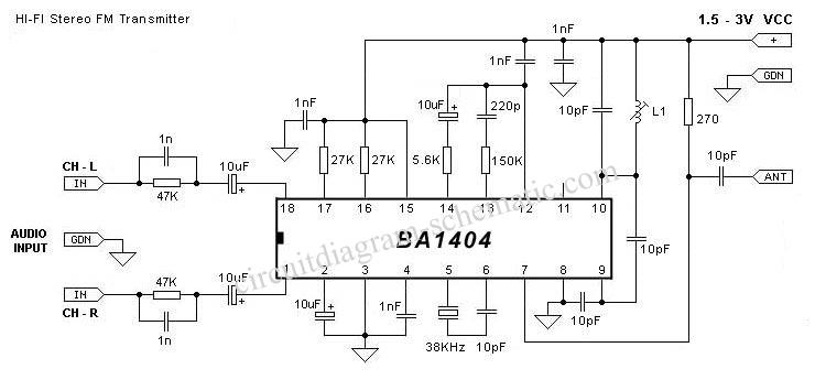
The following circuit illustrates the IC BA1404 used in a stereo FM transmitter circuit diagram. Features include ease of construction, making it accessible for anyone to build. The BA1404 is a versatile integrated circuit designed specifically for FM transmission applications....
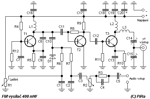
Power supply: 12-14 V stab., 100 mA. RF power: 400 mW. Impedance: 50-75 ohm. Frequency range: 87.5-108 MHz. Modulation: wideband FM. Connect the 6 V / 0.1 A bulb to the output and use R1 to tune the right...

In the transmitter schematic, a ballast resistor is not depicted because most small laser power supplies are typically equipped with an integrated ballast resistor. However, variations in power supply designs may require the addition of an external resistor. In laser...