
Remotely Programmable RTC-Interfaced Microcontroller for Multiple Device Control

The circuit design utilizes an Atmel AT89C52 microcontroller at its core, which is a robust 8-bit microcontroller suitable for embedded applications. It features 32 I/O pins, 4 KB of flash memory, and supports external memory interfacing. The DS12887 RTC chip provides accurate real-time clock functionality, which is essential for time-based control of the devices. The use of a standard Philips TV remote control for programming and controlling the devices adds user convenience, leveraging the widely adopted RC5 protocol for IR communication.
The IR receiver-demodulator TSOP1738 is crucial for receiving the IR signals from the remote control. Its output connects to the interrupt pin of the AT89C52, allowing for efficient handling of commands. The 74LS573 octal latch is employed to store the address and data temporarily, ensuring that the microcontroller can manage multiple peripheral devices effectively. The 8255 PPI facilitates communication with the external devices, providing flexibility in control and data handling.
Overall, the project exemplifies a well-structured embedded system capable of managing multiple devices through precise timing and remote control, making it a versatile solution for various applications requiring automation.This project based on Atmel AT89C52 and Dallas real-timeclock (RTC) chip DS12887 can be used to control and remotely program the switching operation of 24 electrically operated devices. The devices can be switched on/off at precise times repeatedly every day, every month. The microcontroller can be programmed for device control using a normal Phil ips TV remote control. The Philips IR format makes use of RC5 code, which is also known as bi-phase coding. ` In RC5-coded signals (Fig. 2), each bit has a uniform duration. A transition in the middle of the time interval assigned to each bit encodes its logical value (0` or 1`). A high-to-low transition assigns the bit a logic value of 0, ` and a low-to-high transition assigns the bit a logic value of 1.
` We need additional transitions at the beginning of each bit if a stream of equal bits is sent. However, there is no need of additional transitions if the The first two bits are start` bits, which are used to adjust and synchronise the receiver. These bits are used to calculate and analyse the bit length of the other bits. The third bit is a toggle` bit, which is toggled every time a button ispressed at the remote control.
This bit is used to identify whether the button is really pressed or whether an obstacle came in between the IR path of the remote and the IR receiver. The five bits (A4 through A0) immediately following the toggle bit are used to identify the device (see Table III).
So, a maximum of 32 devices can be identified to and respond individually to the same type of coding without any disturbance, i. e. , one among the 64 devices can be identified uniquely. Addresses of some of the remotes are shown in Table III. The six bits (C5 through C0) immediately following the five address bits are the control/command bits.
Therefore a maximum of 64 commands can be equipped in an RC5-type remote. Some of the command codes (decimal equivalents), as used in this project, are shown in Table IV. When any of the command/control buttons on the remote is pressed, the coded signal is received by the IR receiver-demodulator TSOP1738. The output of the IR demodulator circuit is normally high, but when any of the buttons in the remote is pressed, a stream of low-going demodulated pulses will appear at its output.
These pulses are fed to the external active-low interrupt input pin (INT/0) of 89C52. On receipt of the first low-going pulse, the monitor program of 89C52 will get interrupted and jump to the location 0003H, ` where the execution is redirected to receive` sub-routine of the Microcontroller AT89C52 is interfaced to DS12887 (RTC), a 16x2 LCD mod-ule and an 8255 programmable peripheral interface (PPI). The address-decoding circuitry comprises NAND gates 74LS00 and 3-to-8 line decoder 74LS138 as shown in Fig.
1. The interfacing circuitry for the external electrical appliances comprises Darlington array IC ULN2803. The addressing range of various peripheral devices is shown in Table I. In 89C52 (IC1), port P0 is used for outputing multiplexed address (lower8-bit) and data. The address is latched into 74LS573 (IC2) octal latch and RTC DS12887 (IC3) with the help of ALE (address latch-enable) output from pin 30 of IC1.
Only two address lines from IC2 (A0 and A1) have been used for addressing the four registers of 8255 PPI (IC6) in conjunction with the chipselect signal at pin 6 (from IC4) and read/write signals from IC1. Higher-address bits from port P2 of IC1 (A8, A9 and A10 from output pins P2. 0, P2. 1 and P2. 2) are used for generating the chipselect signals from 74LS138 (IC4) cover INg address ranges 000H-0FFH, 100H-1FF and 200- 2FF for RTC, LCD module and PPI chip, respectively.
Quad NAND gate 7400 (IC5) in conjunction with read and write signals from IC1 and chip-select signal from pin 14 of IC4 is used for selecting the LCD module both during read and write cycles of IC1. PPI chip 8255 is configured with port A, port 🔗 External reference
Related Circuits
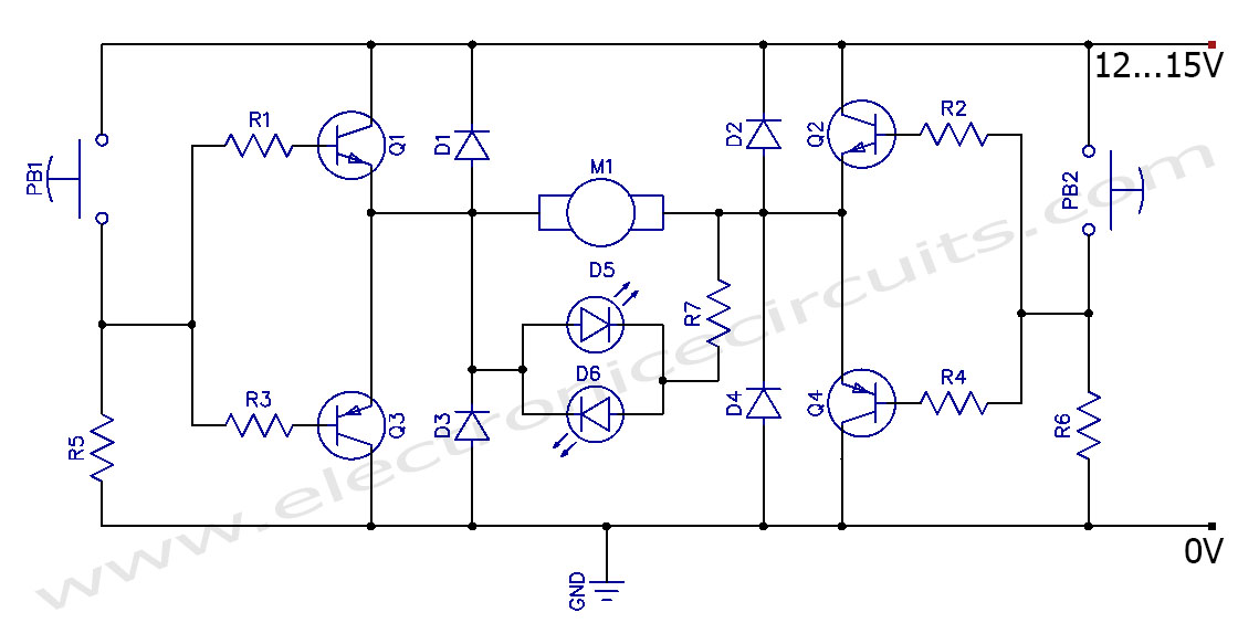
This circuit can control the direction of a DC motor, allowing it to operate in both clockwise and counterclockwise directions (forward and backward). The described circuit employs an H-bridge configuration, which is essential for reversing the polarity of the voltage...
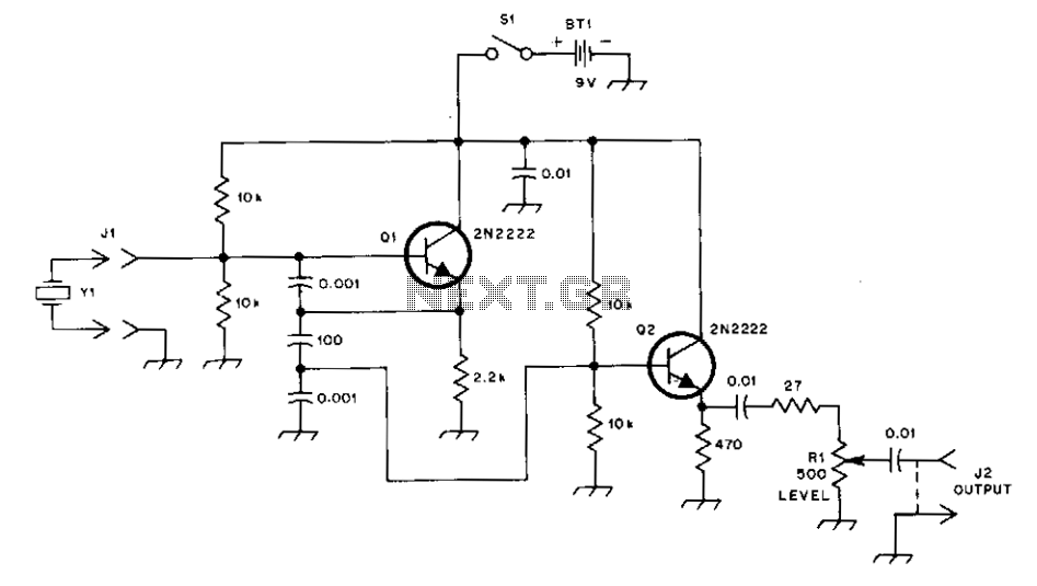
This general-purpose signal source is highly effective for signal-tracing applications. The output level is adjustable, exceeding 1 Vrms into a 50 Ω load. It is compatible with nearly any crystal in the 1 to 15 MHz frequency range. Q1...
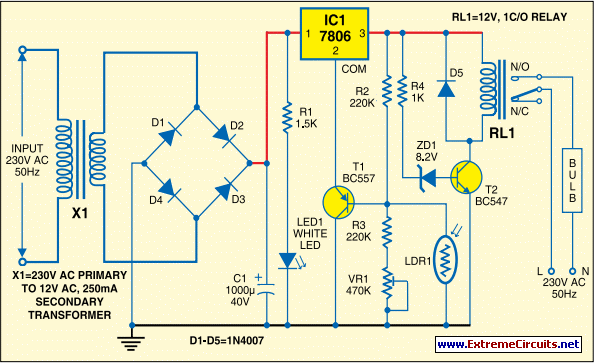
Voltage regulator ICs from the 78xx series deliver a stable output voltage in contrast to a highly variable input supply, provided that the common terminal is grounded. Any voltage applied above zero volts (ground) to the common terminal is...
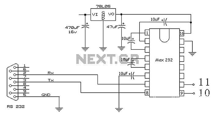
The 51 microcontroller features a full-duplex serial communication port, enabling straightforward serial communication between the microcontroller and a computer. However, certain conditions must be met for effective communication, such as the computer's serial port operating at RS232 levels while...

This 12V wiper speed controller circuit utilizes a 555 timer. It is a straightforward and practical circuit that can be installed in any car. The 12V wiper speed controller circuit is designed to regulate the speed of windshield wipers in...
Test signals inserted in the lines of the vertical blanking interval, defined by the TV standard, e.g. for the 625 standard the CCIR together with the EBU issued the formal specifications for the signals inserted in lines 17, 18,...