
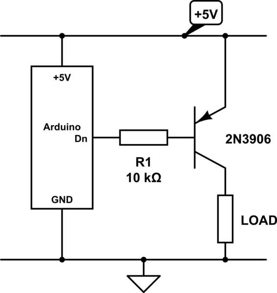
resistors Current flows from the source towards the sink

The circuit utilizes a voltage divider formed by two resistors, R1 (10KΩ) and R2 (5KΩ). The output voltage (Vout) at the junction of these two resistors can be calculated using the voltage divider formula:
\[ V_{out} = V_{in} \times \frac{R2}{R1 + R2} \]
In this case, if the input voltage (Vin) is 5V, the output voltage across R2 (5KΩ) can be calculated as follows:
\[ V_{out} = 5V \times \frac{5KΩ}{10KΩ + 5KΩ} = 5V \times \frac{5}{15} = 3.3V \]
This indicates that the voltage across the 10K resistor (R1) is indeed 3.3V, confirming the intended operation of the circuit. However, it is essential to note that the voltage across the 5K resistor (R2) is 1.7V, which represents the voltage drop when current flows through the resistive path.
The behavior of the circuit relies on the current flow from the voltage source through the resistors and to the GPIO pin. When the current is active, the voltage at the GPIO pin is influenced by the potential divider created by the resistors. The voltage at the GPIO pin is effectively the voltage drop across R2, which is 1.7V.
It is critical to ensure that the GPIO pin can tolerate this voltage without damage and that the current flowing through the resistors does not exceed the maximum ratings for either the GPIO pin or the resistors themselves. This circuit configuration can be effectively used in microcontroller applications where interfacing with higher voltage levels needs to be safely managed, ensuring that the GPIO pins remain within their specified voltage limits.
In summary, the circuit functions correctly as a voltage divider, providing the necessary voltage levels while maintaining safe operating conditions for the GPIO pin.It`s supposed to reduce the max. voltage between the GPIO input pin and the current source to 3. 3V, since 5V * (10K/(10K+5K) = 3. 3V. The thing is - 3. 3V is the voltage over the 10K resistor and 1. 7V is the voltage over the 5K one. As long as the current flows from the source to the sink, the voltage between the source and the GPIO pin should be 1.7V - what am I missing 🔗 External reference
Related Circuits
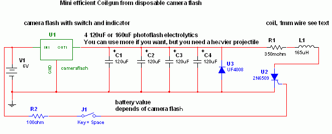
This is a fun and non-dangerous project for individuals interested in launching projectiles using magnetic forces. The mechanism operates by positioning a ferromagnetic projectile at one end of a coil and applying a power pulse. The critical aspect is...
The emitter will consistently be a few hundred millivolts lower than the base voltage in this configuration. With the base voltage set at 5V, the emitter voltage is likely to be around 4.5V, depending on the current drawn by...
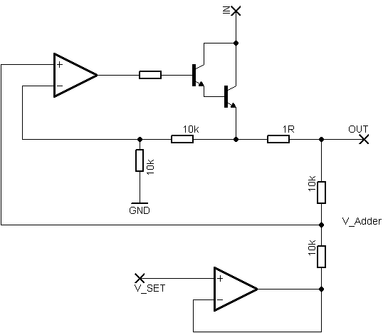
Rsense will cause Q2 to conduct when a threshold of approximately 0.65V is reached. Rbias will determine the extent of this limitation, although this aspect remains unclear. Particularly, if Rsense is positioned on the high side, simply activating Q2...
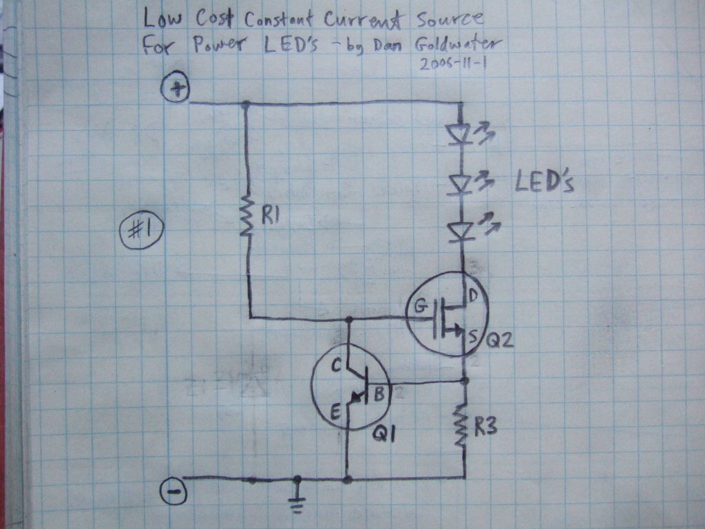
Here is a simple and inexpensive ($1) LED driver circuit. The circuit functions as a constant current source, ensuring that the LED maintains consistent brightness. The LED driver circuit is designed to provide a stable current to the LED, which...
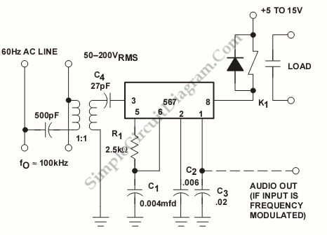
A 567 IC tone decoder/detector can be utilized to construct a remote control or intercom system. This circuit is capable of controlling a relay or transmitting an audio signal. The 567 IC is a versatile integrated circuit designed for tone...

The LTC6101 operational amplifier can be utilized for high-voltage current monitoring and sensing. This circuit is capable of sensing current in a 500-volt system. Here is the schematic diagram. The LTC6101 is a high-voltage current sense amplifier designed specifically for...