
Sawtooth generator circuit a

The complementary sawtooth generator circuit operates by utilizing two transistors (VT1 and VT2) configured in a feedback arrangement to produce a repetitive sawtooth waveform. The circuit's operation begins with the capacitor C in a discharged state, resulting in both transistors being off. As the capacitor charges through resistor Rs, the voltage at point E rises gradually. Once it surpasses the voltage at point A, transistor VT2 turns on, allowing a current path through R3 to the base of VT1. This action causes VT1 to also turn on, creating a feedback loop that drives both transistors into saturation.
The saturation of VT1 and VT2 allows the capacitor C to discharge rapidly, generating the downward slope of the sawtooth waveform. The discharge continues until the voltage across capacitor C falls below a critical value. At this point, the feedback mechanism ceases to maintain the saturation of VT1, and both transistors turn off, ceasing the discharge process. The cycle then repeats as the capacitor begins to charge again.
The choice of component values, including the resistors (R3, R4, and Rs) and the capacitor (C), is crucial for determining the frequency and amplitude of the output waveform. The timing characteristics of the sawtooth waveform can be adjusted by varying these component values. The circuit's design allows for stable operation and reliable waveform generation, making it suitable for applications requiring a sawtooth signal, such as in oscillators, waveform generators, and timing circuits.Application circuit is shown in a complementary sawtooth generator. In the figure, the horse is VT1 base current limiting resistor, the conduction time to prevent excessive bas e current flows through the crystal tube VT1 base, R4 transistor VT2 collector leakage current bleeder resistor to ensure when VT2 end, VT1 reliable cutoff. One under normal circumstances, the power island EJ. When the power is Shu Yi cut turned from no charge in the capacitor C, so both ends of the electric voltage is zero (U0-0), then transistor VT2, the emitter potential is zero, the base potential is A potential point, so UA UE.
Transistor VT2 off. VT1 base also granted without electricity surges, also in an off state. Power capacitor C is charged through the resistor Rs, with the increase in charging time, E point potential has also been on the rise. When the potential at the point E over A point potential, VT2 into the enlarged area, its collector current flows through the resistor R3 VT1 base, VT1 from the same cut-off and into the enlarged area, the collector current through the VT1 VT2 amplified again VT2 feedback to the base, so that the result of positive feedback, forcing VT1, VT2 are saturated.
Capacitor C by saturated transistor VT1, VT2 discharge. With the increase of the discharge time, the voltage of the capacitor C continues to decrease. When the voltage drops to a certain point value E, if the parameters chosen, this time, the base current of transistor VT1 VT1 is not sufficient to maintain saturation, will turn off the circuit by making VT2 positive feedback form for off state, circuit into the second cycle. The output waveform is shown
Related Circuits
The circuit for a transistor tester is a relatively simple device. The transistor tester circuit illustrated below can be utilized to measure and identify the pins of a transistor, as well as determine its condition. Furthermore, this circuit can...
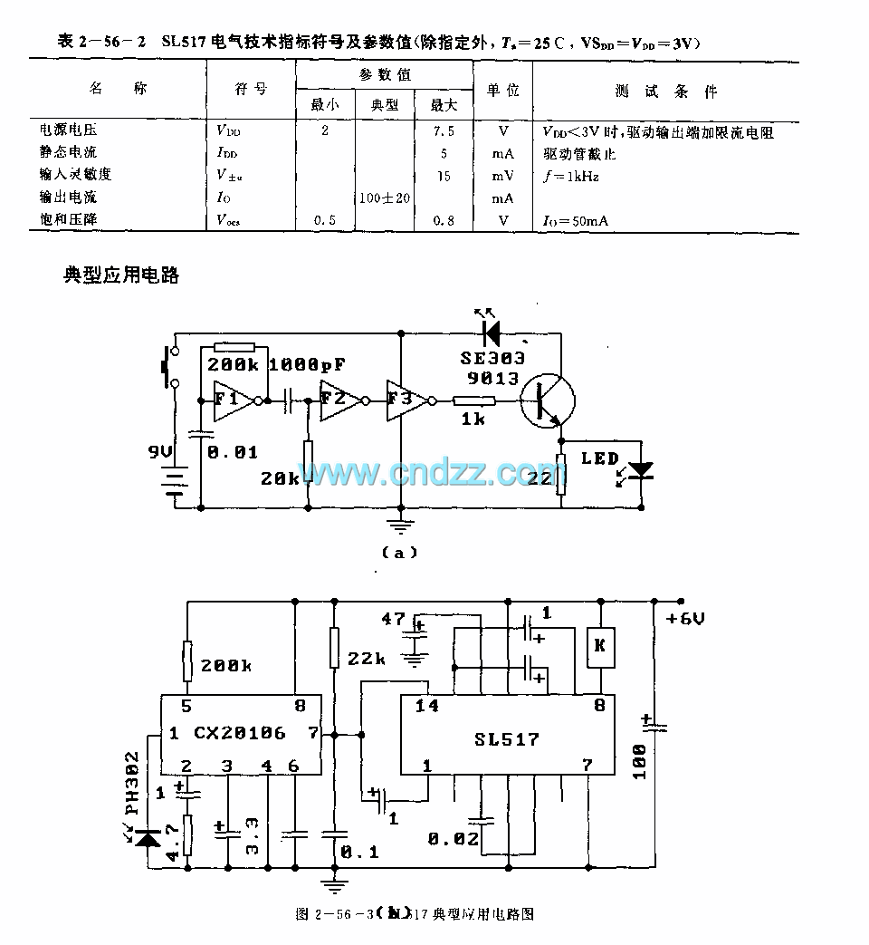
The SL517 is designed as an audio, RF, or infrared decoder circuit suitable for electronic toy applications. The internal circuitry consists of an analog amplifier, a frequency divider, a bistable circuit, and a driver. It utilizes CMOS technology, has...
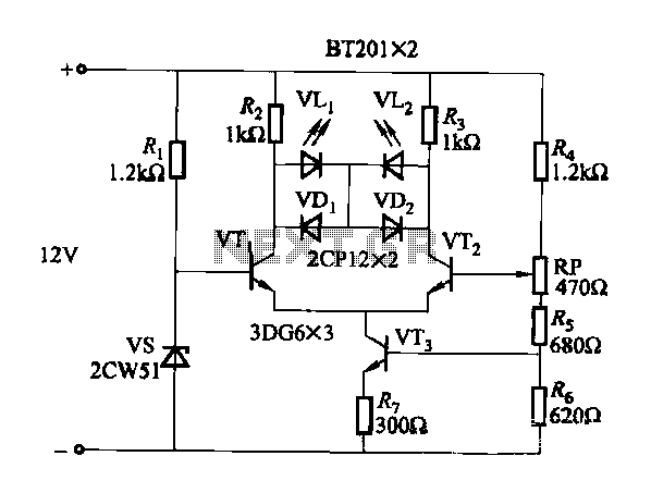
The circuit for monitoring DC power supply under-voltage and over-voltage is depicted in Figure 13-93. It is designed to ensure that the DC power supply voltage remains within normal operating limits. When the supply voltage is at 12V, the...
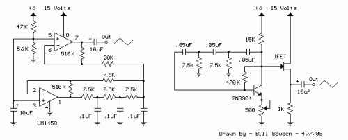
The two circuits demonstrate the generation of low-frequency sine waves by shifting the phase of the signal through an RC network, facilitating oscillation when the total phase shift reaches 360 degrees. The transistor circuit on the right produces a...
This circuit is designed for selective tuning adjustments between two closely spaced audio tones. The frequency of the circuit is determined by the selected capacitors and resistors in the feedback loop between the collector and base of transistor Q1....
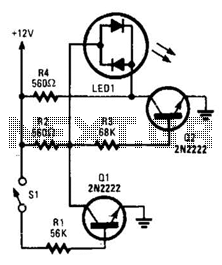
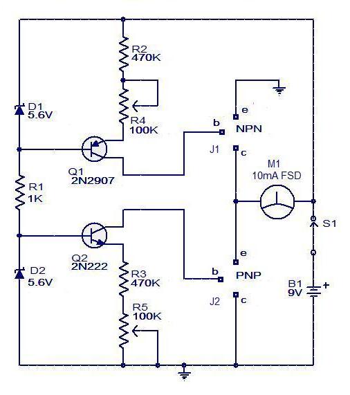
With switch SI open, base bias is supplied to transistor Q2 through a voltage divider formed by resistors R2 and R3, which activates the green element of the LED. This indicates that power is being supplied to the project....