
Schematic diagram for OKI/PDG

The TIQ Flash ADC architecture utilizes a specific row-based configuration to optimize performance and efficiency. Each row is designed to facilitate the conversion of an analog signal into a digital representation, which is crucial for high-speed applications. The comparator within each row plays a pivotal role by comparing the input voltage against reference levels, generating a binary output that indicates whether the input voltage is above or below these levels.
The gain booster is integrated to enhance the signal strength, ensuring that the comparators operate effectively even with low-level input signals. This component is essential for maintaining signal integrity and improving the overall dynamic range of the ADC.
The 0-1 generator is responsible for producing a digital signal output based on the comparator's results. This generator translates the analog input into a binary format, which is then processed further by the connected digital circuitry.
Additionally, the ROM (Read-Only Memory) in each row stores calibration data and reference voltages necessary for accurate conversions. This memory component is critical for ensuring that the ADC maintains precision across various operating conditions.
The stacked row configuration allows for a compact design, reducing the overall footprint of the ADC while maximizing the number of channels that can be integrated into a single device. This design choice is particularly beneficial in applications where space is at a premium, such as in mobile devices or high-density circuit boards.
In summary, the TIQ Flash ADC's layout integrates essential components in a row-based architecture, optimizing performance through careful design considerations, including signal boosting, binary conversion, and data storage, all while maintaining a compact form factor suitable for modern electronic applications.The layout design of the TIQ Flash ADC follows closely with the shown circuit diagram. A row layout is designed, and the rows are stacked. A row consists of a comparator, a gain booster, a 0-1 generator, and a ROM (one row). 🔗 External reference
Related Circuits
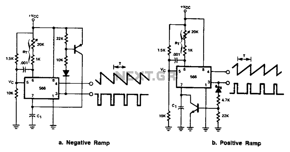
The 566 can be connected to either a positive or negative ramp generator. For a positive ramp generator, an external transistor is driven by the output pin 3. At the end of charging, C1 discharges quickly, allowing for immediate...
The laser torch is an economical device with impressive cost-performance characteristics. Its primary feature is the exceptional performance of the condenser, allowing for an optical range of 1200 to 1500 meters. The beam remains focused and small even at...
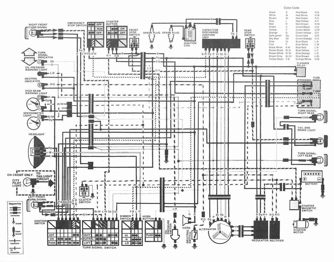
The following image depicts the electrical wiring connection diagram for the Honda Motorcycle CB400 (Hawk II). It illustrates the interconnections between various Honda components, including the turn signal, emergency stop switch, starter button, spark plug, capacitor discharge ignition unit,...

The pre-regulator circuit is connected to a capacitor and a resistor element. The regulator operates in its conducting direction through the input. A capacitor is connected to AC power, and in the blocking direction, it limits the current, allowing...

The 2N388A transistors are inexpensive (approximately 18 cents when purchased in lots of five or more). The 2N5088 transistors are readily available from Mouser. Other components can typically be sourced from Radio Shack or local stores. To convert to...
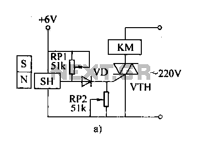
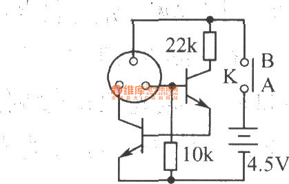
The automatic weapon features a magnetic switch circuit that is simple, reliable, has a low failure rate, and offers good versatility. It can be used for output performance or converted into mechanical displacement applications. The circuit diagram utilizes a...