
Schematics of TTL CPU

The program counter circuit is designed to facilitate the operation of a digital system by managing the sequence of instruction execution. The integration of A-0 to A-3 and B-0 to B-3 into a single 4-bit bus allows for efficient data transfer between the control unit and the program counter. The control circuitry plays a crucial role in interpreting JUMP instructions, which are essential for altering the flow of execution by loading new addresses into the program counter.
During testing, the implementation of pull-up and pull-down resistors is critical for ensuring stable logic levels on the bus lines. These resistors prevent floating inputs, which could lead to unpredictable behavior in the circuit. The choice of a 555 timer for the clock circuit is advantageous due to its ease of use and versatility; however, achieving higher frequencies necessitates careful selection of component values. The adjustable potentiometer allows for fine-tuning of the clock rate, but the duty cycle must be optimized to ensure reliable operation of the counters.
Oscilloscope measurements will provide valuable insights into the clock signal's characteristics, particularly the pulse width and frequency stability. Observations of stalling behavior in the counters beyond 10Hz indicate that the current design may require adjustments to maintain synchronization at higher speeds. Overall, the layout improvements and the focus on testing methodologies will contribute to the successful implementation of the program counter within the broader digital system.I just finished doing the 3rd Eagle layout of the program counter and this one actually makes sense to look at. The first two were a mess of wires intersecting and crossing over each other so that it was hard to see what was connected and what wasn`t.
Hopefully anyone looking at this diagram can follow along and get what I`m aiming for. A-0 to A-3 and B-0 to B-3 are on the same 4-bit bus that connects to the instruction opperand through the control circuitry so that new addresses can be loaded into the program counter through the JUMP instruction. When testing they should have pull-up/down resistors or switches holding them at hi/low. The clock circuit is a simple 555 circuit with an adjustable rate via a potentiometer. It works for now but I have to refine my component values to make it work at speeds higher than about 10Hz.
I suspect that the duty cycle isn`t well balanced related to the frequency. I`ll have to scope it to see what`s really going on but I think the length of the pulse is too short as the clock speeds up because my counters should be able to work at speed but they start stalling when I get going past 10Hz which is pretty slow. 🔗 External reference
Related Circuits
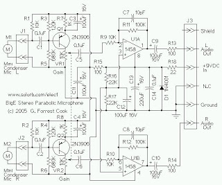
The mini condenser microphone converts sounds into an electrical signal. Resistor R1 provides bias for the condenser microphone's internal amplifier transistor. The 2N3906 PNP transistor acts as a low-noise microphone input amplifier. The 10K gain potentiometer is used for...

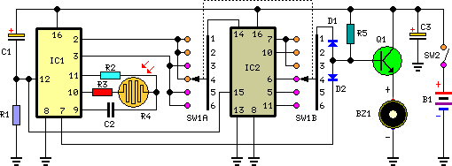
IC1 operates as an oscillator that drives an infrared LED with pulses of 0.8 milliseconds at a frequency of 120 Hz, generating approximately 300 mA of peak current. Diodes D1 and D2 are aligned and positioned a few centimeters...
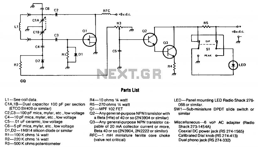
The circuit consists of two fundamental components: the oscillator and the detector. The oscillator employs a Field Effect Transistor (FET) in a Colpitts configuration. The energy circulating within the oscillator's tank is coupled through capacitor C4 to the detector...
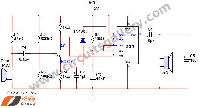
This document discusses a simple project utilizing the 555 timer IC. The 555 timer IC can be configured as an audio amplifier using an astable multivibrator configuration. It performs pulse width modulation (PWM) on an audio signal. The current...
This timer is intended for individuals seeking to achieve a tan while minimizing excessive exposure to sunlight. A rotary switch adjusts the timer based on six categorized photo-types. A photoresistor modifies the preset time value in relation to sunlight...

The 10K resistor is necessary if the receiver is to mute (squelch) under no-signal conditions. An additional 100K resistor can be added in series with this resistor to create an adjustable squelch. This circuit is designed to drive a...