
Selfrunning Free Energy 5 KW Kapanadze 2
Warning: Undefined array key "extension" in /var/www/html/nextgr/view-circuit.php on line 477
Deprecated: strtolower(): Passing null to parameter #1 ($string) of type string is deprecated in /var/www/html/nextgr/view-circuit.php on line 477

The circuit design involves a crystal oscillator that operates with improved efficiency and stability compared to traditional CMOS RC oscillators. By employing a bipolar transistor in the oscillator circuit, the idle current can be minimized, enhancing the overall performance of the system. The oscillator is integrated with the tank circuit formed by inductors L1 and L2, which are crucial for maintaining oscillation. The selection of diode types in the rectifier circuit plays a significant role in reducing voltage losses, thereby improving the efficiency of power delivery to the pump circuit.
The adjustable coupling of the coils allows for optimization of the energy transfer between the tank circuit and the pump oscillator, which is essential for achieving the desired operational characteristics. The implementation of a voltage doubler circuit can further enhance the voltage available for the oscillator, contributing to the overall efficiency of the system. The feedback mechanisms involving the varicap diodes are critical for tuning and stabilizing the oscillator frequency, ensuring that it operates effectively under varying load conditions.
In summary, the circuit aims to achieve a balance between low power consumption and effective energy transfer, with a focus on utilizing advanced components and configurations to optimize performance. The insights gained from the waveform analysis and component specifications provide a foundation for further exploration and refinement of the circuit design, potentially leading to innovative applications in low-power electronics.Trying to estimate the pump input energy your circuit needs, let say your average voltage input (waveform D) is around 6V (12Vpp) and let say your average input current (waveform G) is around 1. 5 - 2mA (8mApp) so to maintain the loaded oscillations in L1-L2 tanks you need about 9-10mW input power (rough and rigorous estimation of course).
This is what roughly the xtal oscillator as its output power should produce instead of the Wavetek gen and the xtal oscillator is to be fed from the tank circuit of course. It was a very good idea to use xtal oscillator to get rid of the supply voltage dependent frequency stability of CMOS RC oscillators and reduce the self-consumption of the oscillator itself.
Here I would refer to an also micropower xtal oscillator with bipolar transistor, maybe its idle current consumption is lower than that of the FET oscillator, this way convertion efficiency may improve, see this link: (the Gate Control Function with the CMOS buffer may be omitted of course and supply voltage can be towards the 5-10V range what the rectifier diodes give, instead of the suggested 3V. ) I understand the definite need for the 50% duty cycle the pump oscillator should produce, sorry for my suggestion on lower duty cycle, my thought was to reduce the ON time for the CMOS RC oscillator, to reduce its power consumption.
Regarding the 5cm OD coils, it is ok but perhaps the coupling coil L3 could be made on a separate card board support of an OD=5. 1cm and you could adjust the coupling of L3 to L1 by sliding L3 over L1, maybe a more optimal position could be found, meaning less load on the tank.
This variable coupling could not be made in case of ferrite pot cores, the solution in that case is to use a multitap coupling coil. The forward voltage loss of the diode bridge can be reduced not only by 4 Ge diodes but by using a full wave voltage doubler which needs only two diodes instead of 4, and if these two diodes are Ge types, you may gain (for free) about 1.
2 to 1. 3V in voltage across the 200uF puffer cap versus the 4 diode bridge. (OF course the voltage doubler in itself is not a power multiplier. ) See this link which doubler I mean: It would be interesting to learn whether you changed the negative bias voltage up and down from its 10V value as shown or you found it as optimum at 10V for the varicap diodes (This 10V source was loaded by the reverse current of the varicap diodes, meaning only a maximum of some 100 nanoAmper load all the time. ) Also I would be curious on the DC resistance of L1 and L2 coils. Your kind and detailed report on this circuit, perhaps combined with my humble suggestions, could inspire some further interest towards achieving a selfrunner at some mW power level.
One would ask what usefulness has a mW power circuit and the answer is: enormous if it selfruns. I`ll cut it short as the following rumblings are completely outside this thread`s target, just allow us to complete only a preliminary check as the matter`s OU implications are to be considered worth of interest. I`ve seen that in order to maintain the down-conversion mode in tank circuit the power needed could be less than you have assumed.
In fact the waveform in TestPoint G due to the small on-screen view is not good. For your use I report here a much detailed waveform that I captured using a wide-band I probe on the pump oscillator return wire. In the upper trace you can appreciate the down-converted 0. 5MHz wave (pump = 1MHz) and the corresponding current pulse delivered by the pump oscillator itself. The +/- spikes have 100mv amplitude and the pulse width is only 20nsec: the required equivalent power is very, very low (The current pulses themselves pass capacitively only trough the back-biased varactor`s capacity).
You have also to add the power delivered by the back bias circuit. that in any case is in the nA range (yes, back bias is a very nice method to change t 🔗 External reference
Related Circuits
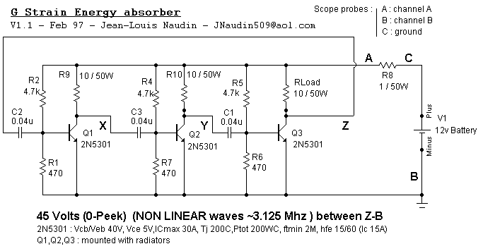
It is important to know that transistors Q1, Q2, Q3 must not work like an astable (tri-phase) multivibrator (you could verify it on scope (no square waves but NON LINEAR wave between XB, YB, ZB must be displayed on...
Convert the smart cards into manual push buttons to control energy consumption, alleviating the consumer's concern about sourcing smart cards, especially given the limited supply in the area. The proposed modification involves replacing the current smart card system with...
Instructions to assemble a small project on wireless energy transfer. If anyone has a simple schematic suitable for beginners, please share or provide instructions. The simplest one found so far is from a Hungarian YouTube channel, but it is...
A current transformer H11-3 needs to be constructed. Select a transformer core with a minimum power rating of 2W for the first secondary winding. Use enameled wire with a diameter of 0.12 mm and wind approximately 1000 turns. The...
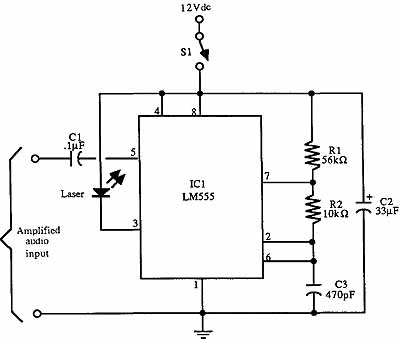
Due to the high frequency of light within the electromagnetic spectrum, it serves as a superior medium for communication compared to radio waves. Lasers are ideal for communication links because they produce a powerful and narrow beam that is...
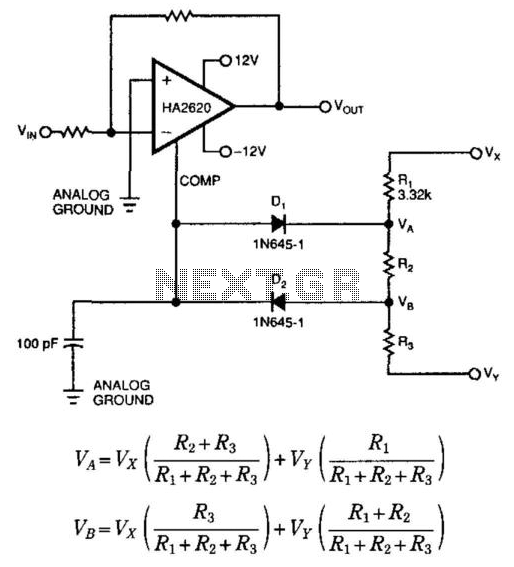
A simple clamping circuit can be added to a Harris 2620 high-speed operational amplifier (op-amp) to create a glitch-free amplifier and clipper. The pin that controls the device's bandwidth is a high-impedance, isolated input, which also tracks the output...