
Simple Audio-Frequency Vco

The sine-wave oscillator operates by utilizing two operational transconductance amplifiers (OTAs), which are configured to generate a stable sine wave output. The frequency of oscillation is directly influenced by the control voltage (U), which can be varied between 0 and 15 V. This adjustable frequency capability allows for versatility in various applications, from low-frequency signals at 6.7 Hz to high-frequency outputs reaching 23.8 kHz.
The output characteristics are designed to maintain low distortion levels, with a maximum distortion of 1% for output signals up to 10 Vpp. Notably, when the output is set to a lower amplitude of 1 Vpp by adjusting potentiometer P1, distortion levels improve significantly to below 0.1%. However, operating the oscillator at output levels below 1 Vpp is inadvisable, as this can lead to instability in the circuit and make it more sensitive to temperature variations.
The configuration of the OTAs includes parallel connections of the Amp-bias inputs (pins 1 and 16), which allows for increased output drive capability, reaching up to 0.75 mA at the output pins (5 and 12). This design choice enhances the oscillator's ability to drive loads while maintaining the desired signal integrity.
To facilitate user control over the frequency output, switch S1 provides a means to select between two distinct frequency ranges. This feature is essential for applications requiring specific frequency outputs, enabling quick adjustments without the need for complex circuitry changes.
It is crucial to note that when adjusting the frequency via the control voltage (Uc), the amplitude setting via P1 must also be appropriately managed to avoid signal distortion. This relationship between frequency and amplitude is fundamental to the oscillator's performance, ensuring consistent and reliable operation across its specified frequency range. The frequency of this sine-wave oscillator is determined by a direct voltage, U" of 0 to 15 V. The distortion on output signals of up to 10 Vpp is not greater than 1 o/o. When the output is reduced with the aid of P1 to 1 Vpp, the distortion drops to below 0.1 o/o. It is not recommended to use output signals below 1 Vpp, because the oscillator then becomes unstable and temperature-dependent. The oscillator consists of two operational transconductance amplifiers (OTAs) contained in one package.
Their Amp-bias inputs, pins 1 and 16, are connected in parallel. These inputs can drive the output currents at pins 5 and 12 to a peak value of up to 0. 75 rnA. Switch S1 enables the oscillator output to be set to two ranges: 6. 7 to 400Hz and 400Hz to 23.8 kHz. The overall range needs a control voltage that varies from 1.34 to 15 V. When the frequency is changed by a variation of Uc and the setting of P1 is not altered, the output signal might be distorted. In other words, the amplitude of the signal must be adapted to the frequency.
Related Circuits
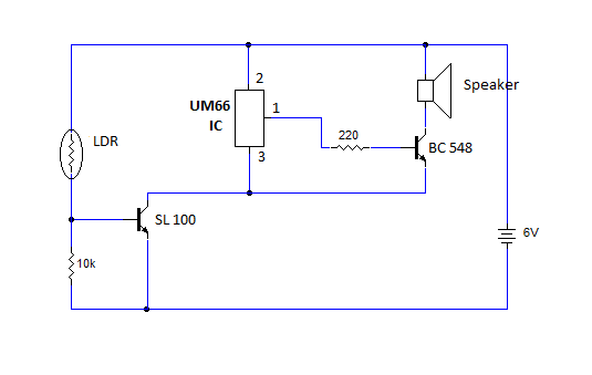
This article provides instructions for creating a light-sensitive morning alarm circuit. The circuit utilizes an LDR (Light Dependent Resistor) or photoresistor to detect morning light, which triggers the alarm section. When light is detected, the circuit produces a melodious...
Simple FM Transmitter Circuit This simple FM transmitter circuit was built using a transistor with a transmission distance of about 300m around your home. The simple FM transmitter circuit utilizes a transistor to modulate audio signals onto a radio frequency...
This design was created to address a challenge with the tailwheel doors of the P-51 Mustang. The issue arises from the complex undercarriage sequence, which would necessitate two independent sequencers. The closing sequence involves the main gear doors opening,...

A few weeks ago, Jason NT7S mentioned the ZL2BMI DSB transceiver as a rig that might be of interest for building. He was correct; it had been seen in SPRAT, but for some reason, it had not been seriously...

This circuit is appropriate for any scenario where over-current protection is necessary. An example from the model train hobbyist community illustrates its importance. Experienced model train enthusiasts understand that locating the source of a short circuit can be quite...

This circuit, based on the NE555 timer IC, toggles the output on and off using a momentary switch. It functions similarly to a mechanical latching relay but resets to its initial state when the power supply is turned off....