
Simple condenser microphone circuit Schematic Diagram

The described circuit represents a simple condenser microphone configuration, where the condenser microphone converts sound waves into an electrical signal. The initial signal is coupled through a 0.1 µF capacitor, which blocks any DC offset, allowing only the AC audio signal to pass through. This is crucial for audio applications, as DC components can interfere with the desired audio signal.
Transistor Q1 operates in a collector-to-base configuration, a common setup for amplifying weak signals. The 470kΩ resistor connected to the base of Q1 plays a vital role in establishing the biasing point of the transistor, ensuring it operates in the active region for optimal amplification. The negative feedback provided by this resistor stabilizes the gain of the transistor, making the circuit less sensitive to variations in temperature and transistor parameters.
The output from Q1 is taken from the collector, where a 3.3kΩ resistor is connected. This resistor is essential for determining the output impedance and plays a role in the overall gain of the circuit. The signal at the collector is then fed into transistor Q2 through another 0.1 µF coupling capacitor. This second capacitor serves a similar purpose as the first, ensuring that the DC biasing of Q1 does not affect the input to Q2.
Transistor Q2 further amplifies the audio signal, which can then be processed or sent to additional circuitry for further amplification or signal conditioning. The overall design of this microphone circuit emphasizes simplicity and efficiency, making it suitable for various audio applications where compactness and reliability are essential. The use of coupling capacitors at both stages is a standard practice in audio signal processing, ensuring that the integrity of the AC signal is maintained while removing any unwanted DC components.The output of condenser mic is coupled via a coupling capacitor of 0. 1 µF, the purpose of this capacitor is to remove DC contents in the audio signal. Transistor Q1 is configured as collector to base biasing mode. This is accomplished via 470k © resistance. This resistor provides negative feedback to the transistor Q1. The output of Q1 becomes a vailable at the collector (across 3. 3k © resistor), which is the input to the transistor Q2 via a 0. 1 µF capacitor. The capacitor removes DC voltages due to the biasing of Q1. You are reading the Circuits of Simple condenser microphone circuit And this circuit permalink url it is 🔗 External reference
Related Circuits

This stereo amplifier utilizes the NE5517/A and features an excellent tracking accuracy of 0.3 dB, which is typical. The offset can be adjusted using the potentiometer, Rp. For AC-coupled amplifiers, the potentiometer can be substituted with two 5.1 k...
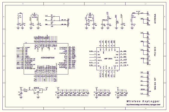
The Wireless Keylogger consists of two main building blocks: the transmitter and the receiver. The actual keylogging takes place in the transmitter, which is in fact a PS/2 hardware keylogger, with a built-in 2.4 GHz wireless module. Captured keystroke...
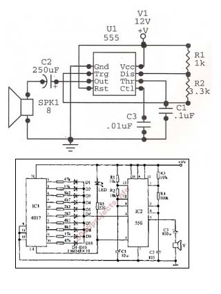
An astable oscillator is constructed using a 555 timer, producing an alarm tone of 1.8 kHz that directly drives a speaker. This fundamental alarm circuit serves as a basis for various other projects in the book. Although the circuit...

This is a design circuit for an alarm. This circuit is intended for an anti-theft wireless alarm that can be used with any vehicle operating on a 6 to 12 volt DC supply system. A mini VHF FM radio-controlled...
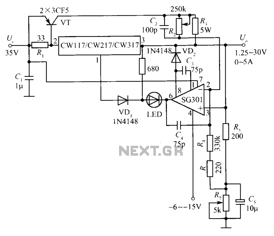
This document presents a diagram of a constant voltage/current power supply box. It is composed of three main components: spread current, constant voltage, and constant current. The design features two 3CF5 power transistors arranged in parallel, functioning as an...
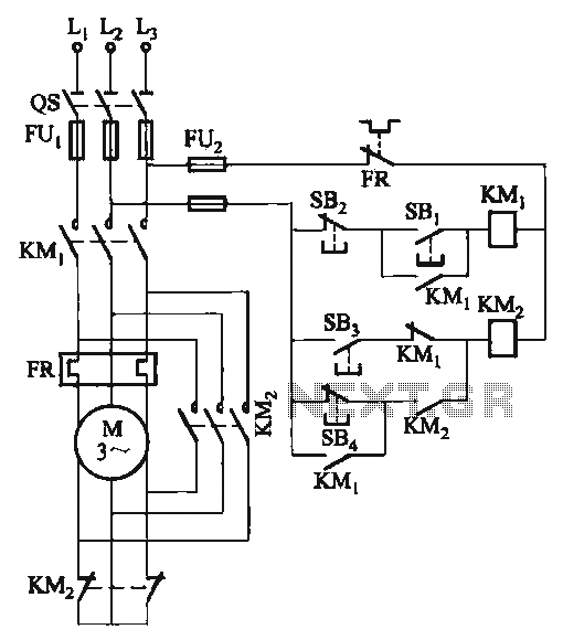
The C620 lathe Y-conversion includes a power-saving circuit designed for controlling the motor's reversing functionality. This system is applicable to machines such as the C620, C630, and CW61100A lathes, as well as radial drilling and milling machines. The C620 lathe...