
Wireless Keylogger circuit

KeeLog has already released one open-source PS/2 hardware keylogger design to the public. Now, it is being done again with the DIY Wireless Keylogger. This design is fully free for private and commercial use, with the following restrictions: All materials presented on this webpage are the intellectual property of KeeLog, and using them constitutes acceptance of the license terms below and the general User Agreement. This Wireless Keylogger project is provided as is, with all faults, and with no warranty whatsoever.
Components
This article describes the entire assembly process of the DIY Wireless Keylogger. Depending on skills, one may choose to create a Wireless Keylogger from scratch or order a preassembled one. A set of components with pre-programmed microcontrollers and standard casing is available, or a fully assembled and tested set of devices.
If one decides to create a Wireless Keylogger, having some basic experience with electronics and soldering is advisable, ideally with SMT (Surface Mounted Technology). The easiest option includes ordering a kit with components and performing the soldering, cabling, and final assembly. This involves having a temperature-controlled soldering iron and good soldering skills. Designing and producing the PCBs requires significant experience and proper equipment.
The table below summarizes the BOM (Bill of Materials) contained in a single transmitter or receiver unit. An additional PS/2 extension cable is required for the transmitter, and a USB type A connector or cable is required for the receiver.
Designator Description Footprint Qty
U1 Microcontroller AT91SAM7S64 TQFP64 1
U2 Transceiver nRF2401 QFN24 1
U3 Voltage regulator MCP1700T-330 SOT-23 1
Q1 Crystal 18.432 MHz HC-49 SMD 1
Q2 Crystal 16 MHz HC-49 SMD 1
R1, R2 Resistor 1.5 kΩ 0805 2
R3, R4 Resistor 27 Ω 0805 2
R5 Resistor 1 MΩ 0805 1
R6 Resistor 22 kΩ 0805 1
C1, C27 Capacitor 10 nF 0805 2
C2, C28 Capacitor 1 nF 0805 2
C3, C4, C6, C7, C8 Capacitor 22 pF 0805 5
C5 Capacitor 33 nF 0805 1
C9 Capacitor 2.2 pF 0805 1
C10, C11 Capacitor 1 pF 0805 2
C12, C22, C23, C24, C25, C26, C32, C33, C34, C42, C43 Capacitor 100 nF 0805 11
C21, C31, C41 Capacitor 1 µF 0805 3
L1 Ferrite Bead 0805 1
L2 Inductor 3.6 nH 0805 1
L3 Inductor 18 nH 0805 1
Both the transmitter and the receiver utilize the same PCB and component set, differing only in cabling and firmware. The Atmel AT91SAM7S64 microcontroller and the nRF2401 wireless transceiver serve as the core components, both requiring specific crystals for stable operation. The MCP1700 voltage regulator ensures proper voltage levels for the system. All other components are passive, including resistors, capacitors, and a few inductors, which support the overall functionality. A simple wire is recommended for the dipole antenna. The design employs a double-sided two-layer PCB, facilitating compact integration and efficient signal handling.The Wireless Keylogger consists of two main building blocks: the transmitter, and the receiver. The actual keylogging takes place in the transmitter, which is in fact a PS/2 hardware keylogger, with a built-in 2.4 GHz wireless module. Captured keystroke data is transmitted through the radio-link in real-time, rather than getting stored.
The receiver on the other hand, is a wireless acquisition unit with a USB interface. All keystroke data received from the transmitter is sent to the host computer via USB. From the software side, this data is available through a virtual COM port, allowing any terminal client to be used for visualizing keystroke data. Familiar with the concept of hardware keylogging? A hardware keylogger is a perfect solution for monitoring user activity, at very low risk of disclosure. A hardware keylogger is a purely electronic device, so no access to the operating system is required, no traces are left, and software has no possibility of detecting such a device.
However, the hardware keylogger concept inherits one weakness: physical access to the keylogger is required for retrieving captured data. This problem has finally found its solution: a Wireless Keylogger. KeeLog has already released one open source PS/2 hardware keylogger design to the public. Now, we are doing it again with the DIY Wireless Keylogger. This design is fully free for private and commercial use, with the following restrictions: All materials presented on this web page are the intellectual property of KeeLog and using them constitutes acceptance of the license terms below and the general User Agreement.
This Wireless Keylogger project is provided as is, with all faults, and with no warranty whatsoever. You should not use the Wireless Keylogger to intercept data you are not authorized to possess, especially passwords, banking data, confidential correspondence etc. Most countries recognize this as a crime. Components This article describes the entire assembly process of the DIY Wireless Keylogger. Depending on your skills, you may choose to create your own Wireless Keylogger from scratch, or order a preassembled one from us.
We can deliver a set of components with pre-programmed microcontrollers and standard casing (as seen on pictures), or a fully assembled and tested set of devices. Please scroll to the kits section for more details. If you decide to create your own Wireless Keylogger, you should have some basic experience with electronics and soldering, ideally with SMT (Surface Mounted Technology).
The easiest option includes ordering a kit with components from us, and doing the soldering, cabling, and final assembly on your own. This involves having a temperature-controlled soldering iron and quite good soldering skills. If you decide to design and produce the PCBs yourself, you should have significant experience in this field and proper equipment.
The table below summarizes the BOM (Bill of Materials) contained in a single transmitter or receiver unit. An additional PS/2 extension cable is required for the transmitter, and a USB type A connector or cable is required for the receiver.
Designator Description Footprint Qty U1 Microcontroller AT91SAM7S64 TQFP64 1 U2 Transceiver nRF2401 QFN24 1 U3 Voltage regulator MCP1700T-330 SOT-23 1 Q1 Crystal 18.432 MHz HC-49 SMD 1 Q2 Crystal 16 MHz HC-49 SMD 1 R1, R2 Resistor 1.5 kΩ 0805 2 R3, R4 Resistor 27 Ω 0805 2 R5 Resistor 1 MΩ 0805 1 R6 Resistor 22 kΩ 0805 1 C1, C27 Capacitor 10 nF 0805 2 C2, C28 Capacitor 1 nF 0805 2 C3, C4, C6, C7, C8 Capacitor 22 pF 0805 5 C5 Capacitor 33 nF 0805 1 C9 Capacitor 2.2 pF 0805 1 C10, C11 Capacitor 1 pF 0805 2 C12, C22, C23, C24, C25, C26, C32, C33, C34, C42, C43 Capacitor 100 nF 0805 11 C21, C31, C41 Capacitor 1 µF 0805 3 L1 Ferrite Bead 0805 1 L2 Inductor 3.6 nH 0805 1 L3 Inductor 18 nH 0805 1 Wireless Keylogger BOM (PDF version) Both the transmitter and the receiver use the same PCB and the same set of components (they differ by cabling and firmware). The Atmel AT91SAM7S64 microcontroller and the nRF2401 wireless transceiver are the core components. Both require crystals for proper operation. Besides the MCP1700 voltage regulator, all other components are passive (resistors, capacitors, and a few inductors).
A simple wire is recommended for the dipole antenna. The double-sided two-layer PCB is shown on the pictures below. 🔗 External reference
Related Circuits
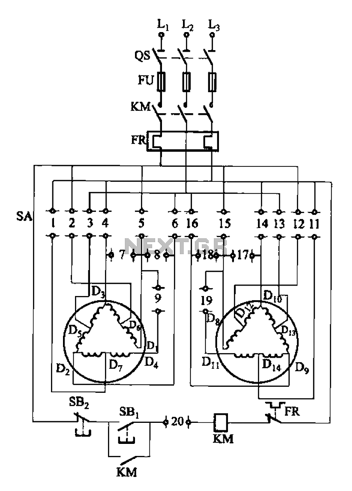
The 3-119 circuit shown in the figure combines switch SA to realize the stator windings, specifically the 2, Y, and 2Y connections, which correspond to the motor speed n1. The 3-119 circuit is designed to facilitate the control of motor...
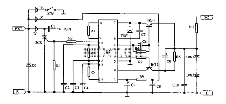
An AC magneto is connected to an external circuit. The output is rectified by diode D1 and stored in capacitor C1. Additional rectification is performed by diodes D4, along with resistors R9 and capacitors C7 and C8, which filter...
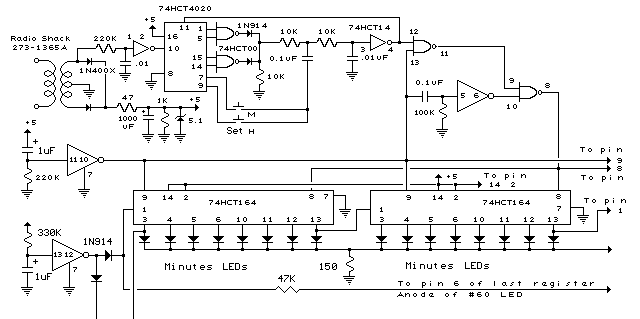
The circuit utilizes 60 individual LEDs to represent the minutes of a clock, along with 12 LEDs to indicate the hours. The power supply and timing circuitry are identical to those described in the previous 28 LED clock circuit....
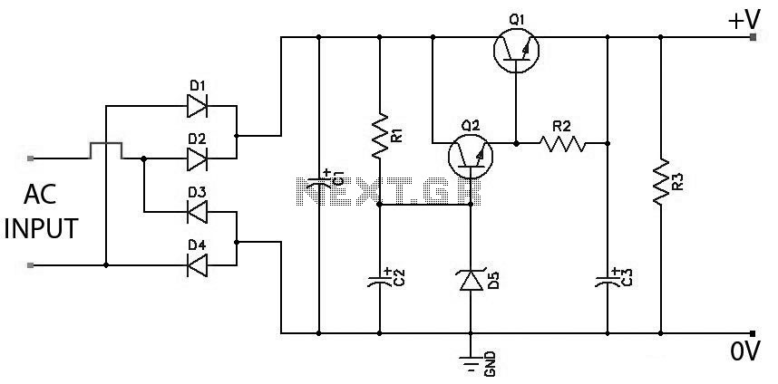
Low Ripple Regulated Power Supply Circuit Diagram. This circuit can be employed in applications requiring high current with minimal ripple voltage, such as in high-powered class AB amplifiers where high-quality audio reproduction is essential. The low ripple regulated power...
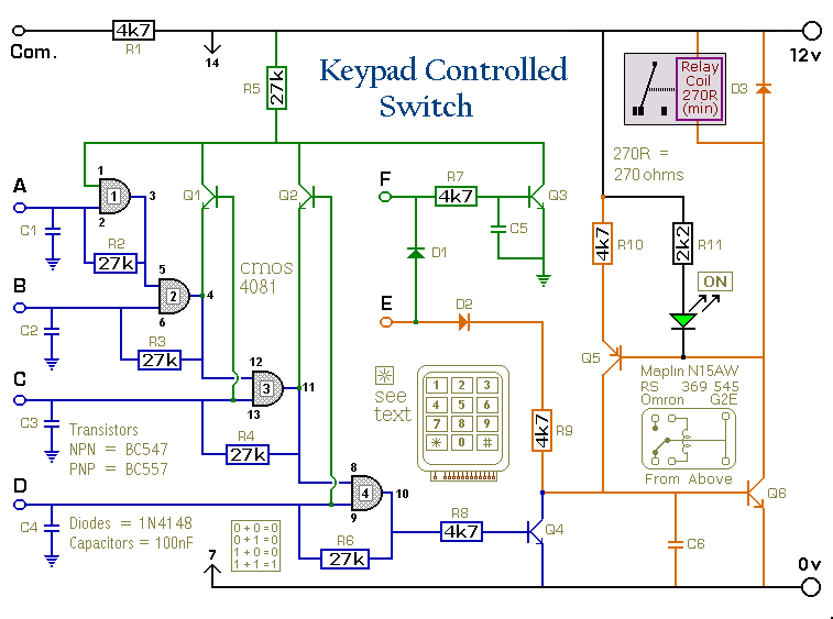
This is a universal version of the four-digit alarm control keypad. The design has been modified to free up the relay contacts, allowing the circuit to function as a general-purpose switch. A single pole changeover (SPCO) or single pole...
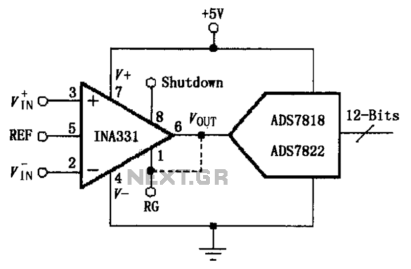
The INA331/332 is configured to directly drive a capacitive input A/D converter. Due to the low output resistance of the INA331/332, it is capable of operating at high frequencies and can directly handle capacitive loads. The output voltage from...