
simple rf id reader module design

The circuit described operates as a basic RFID reader system, utilizing an LC circuit for resonant frequency detection and modulation. The choice of components, including the inductor L1 and capacitor C1, is crucial for achieving the desired resonant frequency of 125 kHz, which is essential for effective communication with passive RFID tags. The use of a low-impedance oscillator ensures that the LC circuit is driven efficiently, enabling the generation of high output voltages that can facilitate reliable tag detection.
The modulation of the output signal is a key aspect of RFID technology, allowing for the transmission of data from the passive tag to the reader. The inclusion of a push-pull output stage enhances the circuit's ability to drive subsequent stages with low output impedance, ensuring minimal signal distortion. The design also incorporates protective elements, such as diodes, to safeguard against potential signal distortion during transitions.
In summary, this schematic represents a fundamental approach to RFID signal processing, highlighting the importance of component selection, circuit configuration, and signal integrity in the design of effective RFID systems. The methodology employed in this design can be adapted and expanded upon for various applications within the field of wireless communication and RFID technology.Used a coil of about 1mH for both sides. Since my chosen frequency was 125 KHz, my capacitor should be 1. 62nF according to the following equation; I picked 1n5 standard value. L1 is driven via a low-impedance 125 KHz oscillator, can be a sine or a square wave since theLC circuit will filter out the unwanted harmonics that are presented in a square wave. If the Q of the inductor is high, then a voltage that is greater than the oscillator`s output is going to be present in the Out . I`ve seen 100 Vpp when I fed the LC circuit with 5Vpp! So, the Out waveform at the top of the C1 is a sine wave of a 125 KHz frequency. Now, the fun thing begins when we put the tag near the reader. L2, C2 pair picks up the 125KHz waveform via L2. So, if you scope C2, you will see 125 KHz sine wave. Now, if you scope Out , you will see that Vpp at C1 will drop when we close the switch SW1. That is because we load L1 ²s magnetic field via L2. Now, push the button like you are sending aMorsecode and watch the Output waveform on the scope. Aha, modulation! Simple! That is how real RFID passive tags work. However, instead of sending Morse code, they modulate the signal with their specific modulation scheme. I am going to work with EM4100 protocol since it is widely used. OK, L1 and C6 are our main guys. They are the components that are mentioned before as L1 ³ and C1 ³ in Figure 1. The circuitry on the left side of L1 is used to drive this LC circuit, and right side of C6 is used to read the changes in the signal.
C1 AC couples the clock signal of 125KHz to the circuit. R1 and R2 biases the transistor Q1. R4 limits its base current. Q1 drives the input of push-pull follower formed by Q2 and Q3. A push-pull follower will drive the signal at low output impedance. D2 and D3 prevents distortions at the cross-overs from zero level. Of course, these measurements are made with the tag almost touching the reader. If we move the tag away about 5 cm from the reader, we may not be able to see the signal even with the oscilloscope. So, we have to filter and amplify this signal and make it ready to be processed by a microcontroller later on.
As you can see above, the signal we are dealing with is an AC signal. To deal with AC signals with the OP-AMPs, you need either a dual supply which goes to negative (for example -12V, +12V), or you need a virtual ground. We are going to assume that half point of our supply voltage is ground. So, if we are using a 5V single supply, our half point is +2. 5V. If +2. 5V is ground, then +5V is our new +2. 5V and 0V is our new -2. 5V. There you have it, a dual supply. We need the output impedance of this supply low, so we use an OP-AMP to buffer the +2. 5V point which is high impedance due to R15 and R16, and we get a low impedance output as shown: OK, now that we have solved that problem, let`s go back to our filter design.
We have a square wave at certain frequency that we want to boost. While boosting the desired frequency we want to kill the other frequencies. But we see a bump there; square wave. A square wave is a signal that includes lots of harmonics (theoretically; infinity) of its actual frequency. These harmonics are hidden in the rise and fall waves, sharper the rise and fall, more the harmonics count.
So, that means, if you low pass filter a square wave -that is not letting higher frequencies to pass a filter, you delete those harmonics and remember, those harmonics are in rise and fall times. Thus, you end up with a sine wave. We do not want that, that`s why we are going to let these frequencies pass as the way they are, however we are going to boost the original frequency.
To do this, we have a filter design like follows: SignalOut is our input coming from the envelope detector. C2 and R3 form a high pass filter to AC couple the input, and D1 protects the non-inverting i 🔗 External reference
Related Circuits
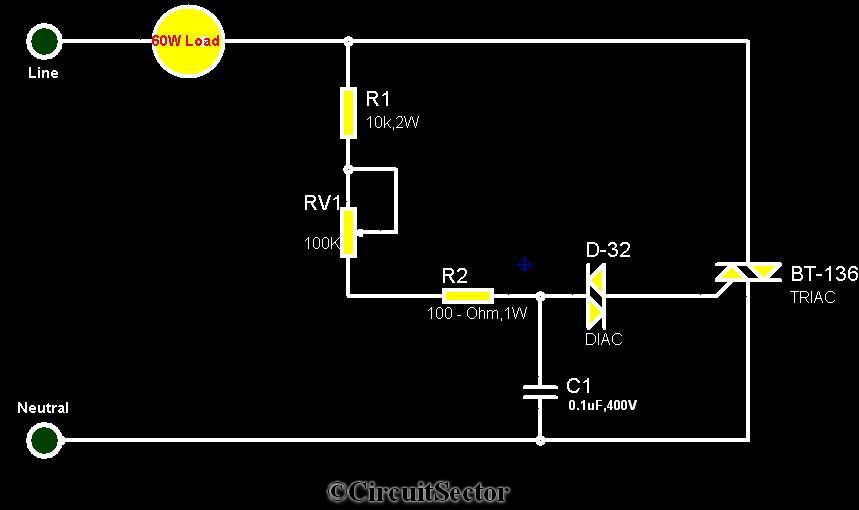
The circuit diagram presented is a triac-diac electronic fan regulator designed to reduce power consumption of electric fans, even at low speeds. Traditional resistor-inductor fan regulators tend to generate excess heat, wasting energy when the fan operates at lower...
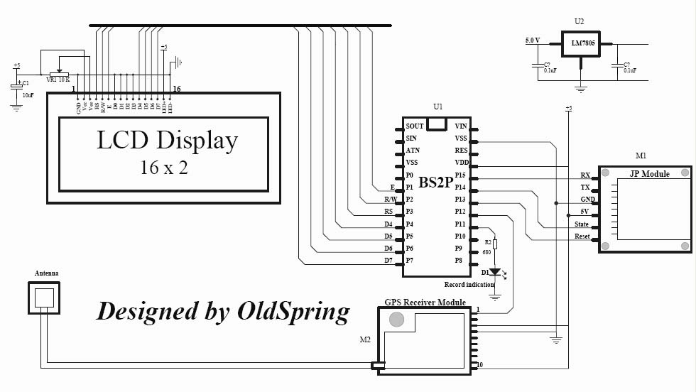
A GPS tracker demonstration program with data logging capability. It utilizes a BasicStamp 2P (or alternatively, a PIC chip) to interface with a GPS module, a JP module, and a 16x2 LCD display. The sample code employed is standard...
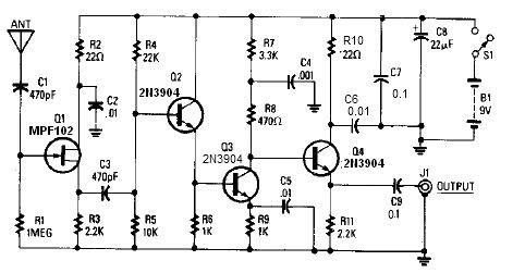
A simple active antenna can be designed using this electronic circuit diagram. This active antenna utilizes transistors and a few common electronic components. In the practice of short-wave frequency reception, a general rule is that a longer antenna will...
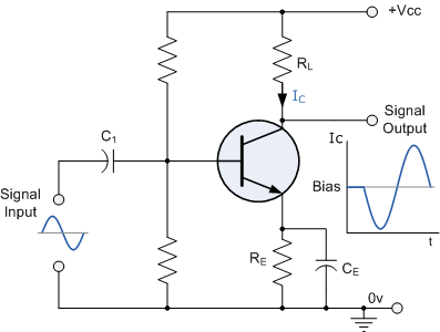
Construct a basic audio amplifier utilizing transistors. While integrated circuit (IC) designs are available for this purpose, the intention is to use transistors to gain practical knowledge about their amplification capabilities. The article "Amplifier Basics - How Amps Work...
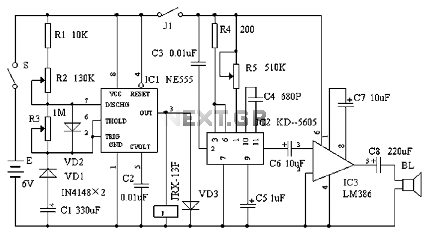
Cats are natural predators of rats, and the use of electronic devices to simulate meowing sounds as a repellent is an effective method. These electronic devices can produce meowing sounds at various frequencies and intervals, making them suitable for...
This tester is designed for tracing wiring on Printed Circuit Boards (PCBs). Resistors below 50 ohms function as a short circuit, while those above 100 ohms behave as an open circuit. The circuit comprises a simple multivibrator activated by...