
simple supply voltage monitor

The described voltage monitoring circuit employs a straightforward design that leverages the characteristics of bipolar junction transistors (BJTs) to provide a reliable indication of supply voltage integrity. The circuit operates within a dual voltage range, monitoring both positive and negative supply lines, specifically ±5 V and ±12 V. The configuration includes two primary transistors, T1 and T3, which are configured as current sources, ensuring stable operation across varying load conditions.
Resistors R1 and R2 play a crucial role in setting the reference voltage drop across the circuit, calculated to be 6.3 V. This voltage drop is essential for maintaining the necessary biasing conditions for the transistors. The current flowing through these resistors is measured at 6.3 mA, which is adequate to activate diode D1 under normal operating conditions, indicating that all monitored voltages are present.
In the event of a failure in the 5 V supply line, the circuit is designed to respond effectively. Transistor T3 continues to conduct, maintaining its state; however, the failure impacts transistor T2's base-emitter junction, which loses its bias. As a result, T2 ceases to conduct, interrupting the current flow through diode D. This change serves as an indication of the fault condition, effectively signaling that one of the critical supply voltages is no longer available.
Overall, this voltage monitoring circuit provides a robust and efficient solution for ensuring the integrity of ±5 V and ±12 V supply lines, utilizing minimal components while maintaining clear operational functionality. The design's simplicity enhances reliability and reduces potential points of failure, making it suitable for various applications in electronic systems where voltage monitoring is essential.A circuit for monitoring supply voltages of ±5 V and ±12 V is readily constructed as shown in the diagram. It is appreciably simpler than the usual monitors that use comparators, and AND gates. The circuit is not intended to indicate the level of the inputs. In normal operation, transistors T1 and T3 must be seen as current sources. The drop acr oss resistors R1 and R2 is 6. 3 V (12 5 0. 7). This means that the current is 6. 3mA and this flows through diode D1 when all four voltages are present. However, if for instance, the 5 V line fails, transistor T3 remains on but the base-emitter junction of T2 is no longer biased, so that this transistor is cut off. When this happens, there is no current through D which then goes out. 🔗 External reference
Related Circuits
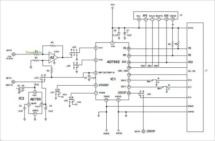
This data sheet describes the evaluation board for the AD9834 direct digital synthesizer (DDS). The AD9834 is a numerically controlled oscillator that utilizes a phase accumulator, a sine look-up table, and a 10-bit DAC. The AD9834 can operate with...
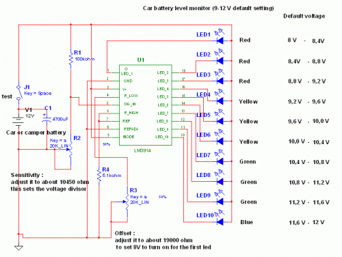
This circuit utilizes the widely available LM3914 integrated circuit (IC). The LM3914 is straightforward to operate, does not require external voltage regulators due to its built-in voltage regulation, and can be powered by a variety of sources. The LM3914 is...
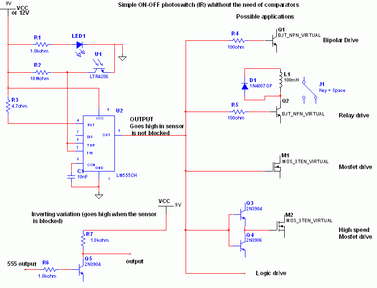
The 555 timer is recognized as one of the most versatile and widely used integrated circuits globally. One of its potential applications is as a simple inverting Schmitt trigger. The 555 timer can be configured in various modes, including monostable,...
The loop antenna L1 is utilized for emission and also functions as the oscillation coil. The high-frequency current flowing through the antenna is synchronized in resonance with the oscillation frequency, ensuring optimal emission performance. Practical applications indicate that the...
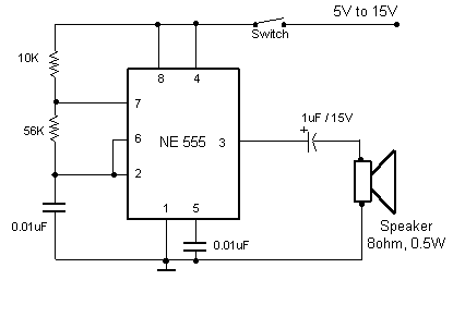
This very simple circuit just uses a couple of resistors, a capacitor and the easily available 555 timer IC. The 555 is setup as an astable multivibrator operating at a frequency of about 1kHz that produces a shrill noise...
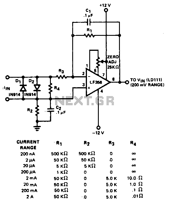
The converter features eight decades of current range. The circuit is intended to be used with the 200 mV range of a DVM. The described converter circuit is designed to accommodate a wide range of current measurements, spanning eight decades....