
sine wave to ttl converter

The circuit operates by utilizing a common-emitter transistor configuration, which is well-suited for signal amplification and switching applications. The biasing arrangement formed by resistors R3 and R5 is critical for establishing the correct operating point of the transistor, allowing it to function effectively within the desired frequency range. When a sinusoidal input signal is applied, the transistor amplifies the signal, converting it into a rectangular waveform suitable for TTL logic levels. The transition from sinusoidal to rectangular signals is facilitated by the inherent switching characteristics of the common-emitter configuration, which provides a rapid response to changes in the input signal.
The selection of resistors R6 is important for maintaining the integrity of the input signal. By keeping the input resistance at approximately 50 ohms, the circuit minimizes reflections and signal degradation that can occur when long coaxial cables are used. This is particularly important in high-frequency applications, where signal integrity is paramount. The ability to omit R6 in certain circuit configurations allows for flexibility in design, accommodating various input signal conditions without compromising performance.
Overall, this circuit serves as an effective solution for converting sinusoidal signals to TTL levels, making it suitable for a range of applications in digital electronics and signal processing. Its design considerations ensure robust operation across a wide frequency spectrum while maintaining signal fidelity.The present circuit is intended to convert sinusoidal input signals to TTL output signals. It can handle inputs of more than 100 mV and is suitable for use at frequencies up to about 80 MHz. Transistor T1, configured in a common-emitter circuit, is biased by voltage divider R3 R5 such that the potential across output resist or R1 is about half the supply voltage. When the circuit is driven by a signal whose amplitude is between 100 mV and TTL level (about 2 V r. m. s. ), the circuit generates rectangular signals. The lowest frequencies that could be processed by the prototype were around 100 kHz at an input level of 100 mV, and about 10 kHz when the input signals were TTL level. Resistor R6 holds the input resistance at about 50 , which is the normal value in measurement techniques.
It ensures that the effects of long coaxial cables on the signal are negligible. If the converter is used in a circuit with ample limits, R6 may be omitted, whereupon the input resistance rises to 300 . 🔗 External reference
Related Circuits
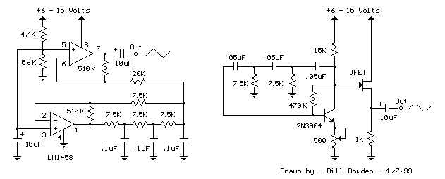
The two circuits below illustrate generating low frequency sinewaves by shifting the phase of the signal through an RC network so that oscillation occurs where the total phase shift is 360 degrees. The transistor circuit on the right produces...
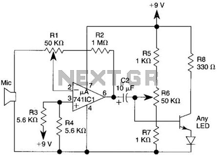
This transmitter utilizes a 741 operational amplifier as a high-gain audio amplifier, which is activated by a microphone. The output of the 741 is connected to Q1, functioning as the driver for an LED. Potentiometer R1 serves as the...
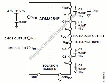
The ADM3251E is a transceiver that features high-speed operation, 2.5 kV full isolation, and a single channel for RS-232/V.28 communication. This device operates from a single 5 V power supply. The ADM3251E transceiver is designed for robust communication in environments...
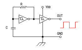
The hysteresis characteristic indicates that the voltage level transitions to high (H) when the input voltage of the inverter rises from 0 V, and the voltage level transitions to low (L) when the input voltage descends from +5 V....
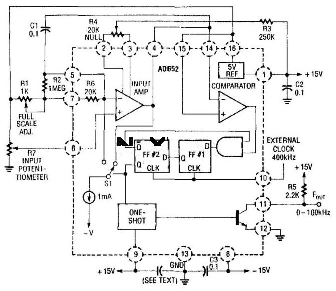
In this application, an AD652 integrated circuit (IC) is utilized in a synchronized voltage-to-frequency (V/F) converter that takes its input from the position of a potentiometer. This setup can represent the position of a mechanical component, weight, size, etc.,...
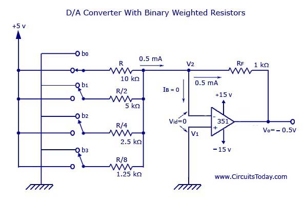
A digital-to-analog (D/A) converter utilizing binary-weighted resistors is illustrated in the accompanying figure. In this circuit, the operational amplifier (op-amp) is configured in inverting mode, although it may also be arranged in non-inverting mode. The schematic represents a 4-bit...