
Single Cell Battery 1.5V 20dB Inverting Amplifier

The amplifier circuit is designed to operate with minimal power consumption, making it suitable for battery-powered applications or low-power devices. The specified total current consumption of 675 nA indicates that the circuit is optimized for efficiency, which is particularly important in portable electronics where battery life is a critical factor.
The output voltage swing of 300 mV peak-to-peak signifies the range of output voltage that the amplifier can provide, which is essential for ensuring that the signal can be adequately processed by subsequent stages in the system. A gain of 20 means that the amplifier increases the amplitude of the input signal by a factor of 20, allowing for effective signal amplification without significant distortion.
In practical applications, the amplifier may utilize operational amplifier (op-amp) configurations, possibly in an inverting or non-inverting setup, depending on the desired signal processing characteristics. The low power consumption is typically achieved through the use of advanced semiconductor technologies, such as CMOS or BiCMOS, which facilitate low-voltage operation while maintaining high input impedance and low output impedance.
The design may also incorporate feedback mechanisms to stabilize the gain and improve linearity, ensuring that the amplified output remains faithful to the input signal. Additionally, the circuit layout should consider minimizing parasitic capacitances and inductances, which can affect performance, particularly at higher frequencies.
Overall, this amplifier circuit represents a balance between low power operation and effective signal amplification, making it ideal for modern electronic applications that require efficiency and reliability.Featuring very low power consumption, 675 nA is the total current? consumption for this amplifier? circuit. The output voltage swing is 300 mVpp with a 20. 🔗 External reference
Related Circuits
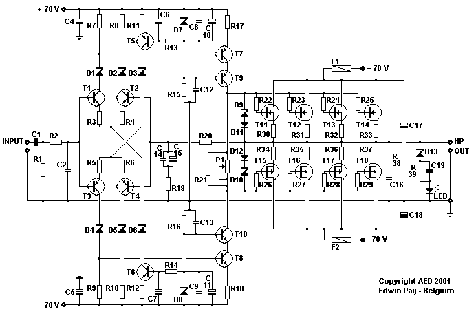
Here I propose a project of an AB class power amplifier, at its simplest, assembled with common components (not very expensive), based on traditional diagrams: a symmetrical differential input stage, a cascode stage driver, and a MOSFET output stage....

A common collector amplifier circuit structure and its key components are outlined. The composition of the common collector amplifier circuit is fundamentally similar to that of a common emitter amplifier circuit, with two notable exceptions: one is the collector...
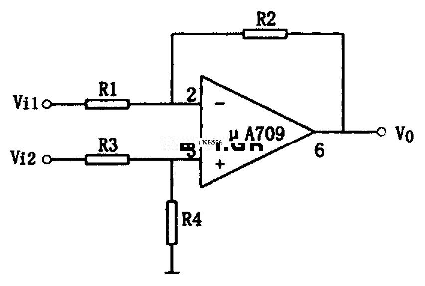
The simple differential amplifier circuit consists of two input signals, Vi1 and Vi2, which are connected through resistors R1, R3, and R4, forming a voltage divider circuit at the op-amp input. Vi1 is applied to the inverting input of...
Camping today often requires carrying various electronic devices for daily activities and entertainment. Typically, a charged lead-acid battery and a power inverter are utilized to ensure a well-organized trip, allowing family members to use their electronic devices comfortably. It...
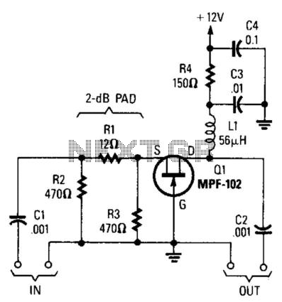
Using an MPF102 JFET, this circuit has a 50-ohm input impedance. The load impedance should be approximately 470 ohms. A 3:1 matching transformer can be utilized to return the impedance to 50 ohms. This circuit will exhibit a gain...
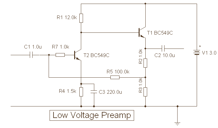
The provided description pertains to a unique low voltage variant of an audio preamp. The emitter voltage of T1 is biased close to half the supply voltage, which is 1.5V. This biasing allows for the maximum output voltage swing. The...