
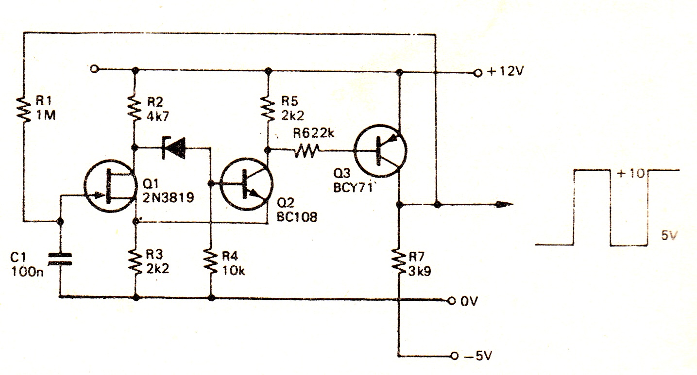
Square-wave generator circuit

The circuit utilizes transistors T1 and T2 to create an oscillator, where the interaction between these two components generates a continuous oscillation. T3 acts as a buffer or amplifier, ensuring that the output signal is at an appropriate level for further processing or utilization.
The high-pass filter, composed of capacitors C3 and C4 along with resistors R6 and R7, is designed to allow higher frequency signals to pass while attenuating lower frequencies. This filtering action is essential for shaping the frequency response of the oscillator circuit, ensuring that only the desired oscillation frequencies are amplified and outputted.
Conversely, the low-pass filter serves to eliminate higher frequency noise from the signal, providing a cleaner output. The combination of these filters allows for precise control over the frequency characteristics of the circuit. The output of these filters is coupled to the base of T3 via capacitor C6 and resistor R8. The capacitor C6 blocks any DC component, allowing only the AC oscillation to control the base of T3.
At the collector of T3, the circuit produces a square wave oscillation signal, which can be used for various applications such as clock generation, signal modulation, or as a timing reference in digital circuits. The design ensures stability and reliability in the output signal, making it suitable for integration into larger electronic systems.T1 and T2 in the circuitform theinherent oscillator, T3 is output level. Network consists of high-pass filter (C3, C4, R6 + - R7) and low pass filter, it`s output is added to the T3 base via C6 and R8, and in the collector of T3, it willget required square wave oscillation signal.. 🔗 External reference
Related Circuits
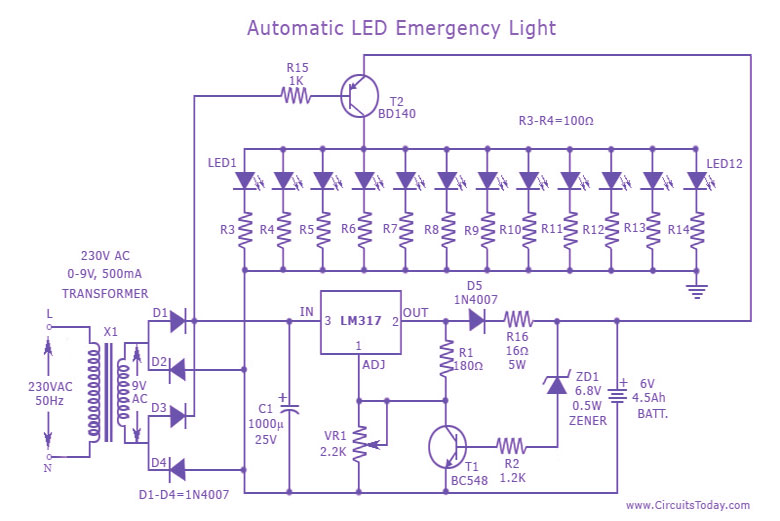
This is a cost-effective and straightforward emergency light circuit developed for CircuitsToday. It is an automatic emergency lamp with daylight sensing capabilities, meaning it detects darkness and turns on automatically, while also sensing daylight to turn off. The circuit...
The circuit employs a field-effect transistor (FET) at the input of a Schmitt trigger, allowing the use of a low-value capacitor. The trigger, controlled by Q1 and O2, exhibits a hysteresis of approximately 3V, regulated by a 3V zener...
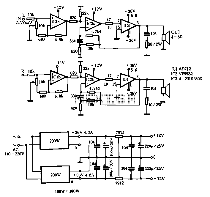
The T amplifier circuit schematic section is illustrated in Figure 3-51. It utilizes the Japan Sanyo STK6303 Pina, which is a high-power thick film integrated circuit. The maximum power supply voltage is 36V, and the output current can reach...
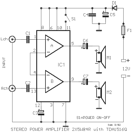
A simple stereo amplifier with minimal external components. It utilizes only one operational amplifier, which is capable of delivering an output power of 2x5W into a 4-ohm load, with a distortion of 0.5%. This stereo amplifier circuit is designed to...
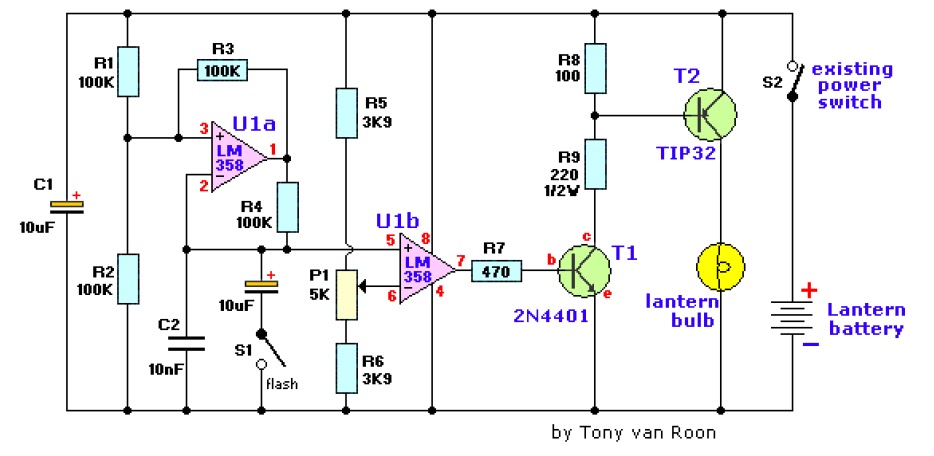
The electronic lantern control circuit enhances an existing battery-powered lantern or flashlight, or can be incorporated into a custom design, by providing high-efficiency dimming and flashing capabilities. This circuit is particularly useful in automotive applications, serving as an effective...
Logic Gates FM Transmitter Circuit Electronic Circuit Schematic Wiring Diagram. The FM transmitter circuit utilizing logic gates is a fundamental electronic design that operates by modulating a carrier frequency with an audio signal. This circuit typically consists of various logic...