
Switch-Mode Voltage Regulator

The switch-mode power supply circuit is designed to optimize efficiency while providing reliable voltage regulation. The MAX638CPA integrated circuit serves as the core of the regulator, facilitating the conversion process with minimal external components. The choice of components is critical; for instance, the inductor L1 and capacitor C3 form a low-pass LC filter that smooths out the output voltage, ensuring that the 5 V supply is stable and free from high-frequency noise generated during the switching process.
The feedback mechanism is crucial for maintaining the desired output voltage. The internal error detector continuously monitors the output voltage and compares it to a precise reference voltage. If the output voltage deviates from the specified 5 V, the FET is modulated to adjust the energy transfer to the load, thereby maintaining regulation. This feedback loop is essential for adapting to varying load conditions, ensuring that the output remains consistent under different operational scenarios.
The low battery indicator feature enhances the usability of the power supply by providing a visual alert when the input voltage approaches a critical threshold. This is particularly useful in battery-powered applications where monitoring the battery state is essential for preventing unexpected shutdowns.
Overall, this switch-mode power supply design exemplifies a balance of efficiency, simplicity, and functionality, making it suitable for various applications where reliable voltage regulation is required. The careful selection of components and the integrated features of the MAX638CPA contribute to the overall performance and reliability of the circuit. Switch-mode power supplies offer the benefit of a much greater efficiency than obtainable with a traditional power supply. The switch-mode regulator presented here has an efficiency of around 85%. An input voltage of 12 to 16 Vdc is converted into a direct voltage of exactly 5 V. The use of a MAX638CPA enables the design and construction of the regulator to be kept fairly simple: only nine additional components are needed to complete the circuit. Resistors RI and R2 are used to indicate when the battery voltage becomes low: as soon as the voltage on pin 3 becomes lower than 1.3 V, D1 lights.
With values as shown for the potential divider, this corresponds to the supply voltage getting lower than about 6.5 V. The output of the IC is shunted by a simple LC filter formed by LI, C3 and D2. The oscillator on board the IC generates a clock frequency of around 65 kHz and drives the output transistor via two NOR gates.
The built-in error detector, the "battery low" indicator or the voltage comparator can block the clock frequency, which causes the transistor to switch off. The IC compares the output voltage of 5 V with a built-in reference (FET). Depending on the load, the FET will be switched on for longer or shorter periods. The maximum current through the FET is 375 mA, which corresponds with a maximum output current of 80 mA.
Related Circuits
The TRF1115 is the first of two ASICs utilized in the receiver section of the Texas Instruments MMDS/MDS/WCS/802.16x chipset. This device is responsible for down-converting the input frequency to an intermediate frequency (IF) within the range of 420 MHz...
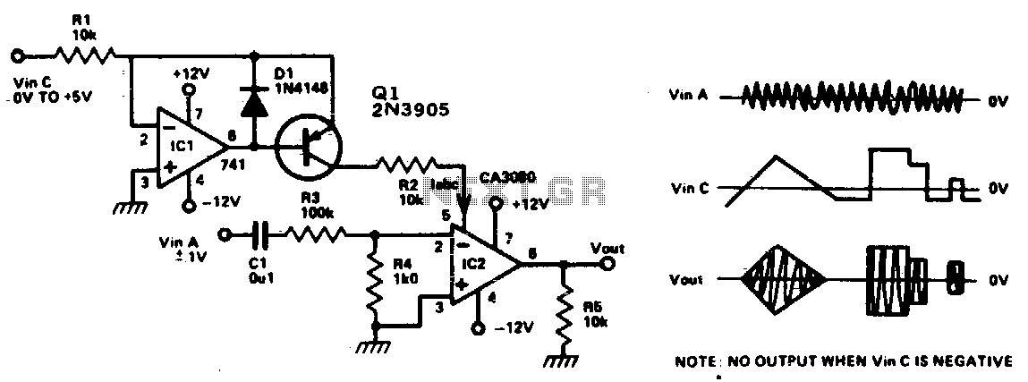
This circuit is essentially an operational amplifier (op-amp) with a differential input voltage of ±10 mV between pins 2 and 3, along with an additional input at pin 5. A current (Iabc) is injected to control the current at...

An Over Voltage Protector is a straightforward circuit designed to safeguard appliances from excessive voltage. It includes a circuit diagram and a parts list for various electronics projects related to over voltage protection. The Over Voltage Protector circuit typically employs...
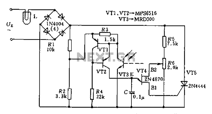
The circuit is designed to stabilize the brightness of lamp L using a thyristor-based AC automatic voltage regulator. The thyristor T5 is connected diagonally across the bridge circuit. The trigger pulses are generated by components VT1, VT2, and VT3,...
For hobbyists or professional electronic engineers engaged in various electronic experiments, troubleshooting, or testing, it is essential to provide a wide range of variable options. In electronic engineering, the ability to manipulate and measure a wide range of variables is...
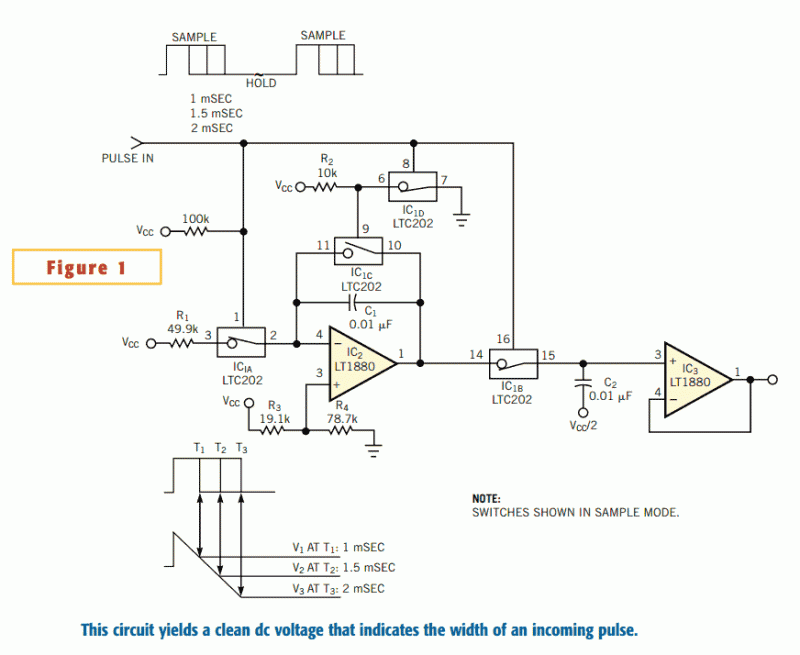
The circuit in Figure 1 converts pulse information to a clean dc voltage by the end of a single incoming pulse. In another technique, an RC filter can convert a PWM signal to an averaged dc voltage, but this...