
Switching Improves Regulator Efficiency

The circuit operates by utilizing a combination of a full-wave center tap (FWCT) rectifier and a full-wave bridge rectifier configuration to optimize the efficiency of the voltage regulation process. The central component, SCR D6, acts as a switch that toggles between these two configurations based on the voltage levels detected at the regulator output.
In the FWCT mode, with SCR D6 turned off, diodes D1, D2, and D5 conduct, allowing the circuit to convert the AC input voltage into a pulsating DC voltage. This configuration generates an output voltage of approximately 17 V, which includes a ripple component due to the nature of rectification. The pulsating DC voltage is fed into the voltage regulator, which is responsible for maintaining a stable output voltage.
The voltage drop across the regulator is critical as it provides the necessary base drive to transistor Q2. When Q2 is active (turned on), it prevents Q1 from conducting, effectively keeping SCR D6 off and maintaining the FWCT operation. This mode is efficient under normal load conditions, as it minimizes power dissipation within the regulator.
However, if the load demand increases and the output voltage of the regulator falls below a threshold of approximately 3 V, Q2 will deactivate. This action allows Q1 to turn on, which in turn activates SCR D6. Once D6 is on, the circuit transitions to the full-wave bridge configuration utilizing diodes D1 through D4. This configuration provides a more robust output by allowing current to flow through all four diodes, ensuring that the output voltage remains stable even under varying load conditions.
The switching mechanism between the two configurations enhances the circuit's overall efficiency and reliability. By dynamically adjusting the rectification method based on the output voltage, the design minimizes losses and optimizes performance across a range of operational scenarios. This approach is particularly beneficial in applications where maintaining a stable voltage is critical, such as in power supplies for sensitive electronic devices. In this circuit, a full-wave bridge is switched to a full-wave center tap to reduce regulator dissi pation. SCR D6 switches between configurations. When D6 is off, the circuit is an FWCT rectifier using Dl, D2, and D5. It applies 17 V plus ripple to the regulator input. The drop across the regulator supplies base drive to Q2. If Q2 is on, Ql is off, and D6 is off. If the regulator voltage drops below about 3 V, Q2 turns off, and turns Ql on, which turns on D6. This changes the circuit to an FW bridge using Dl through D4.
Related Circuits

Before designing an adjustable voltage regulator into a circuit or performing a redesign, it is necessary to calculate the values for two resistors. While this process is straightforward, sourcing the appropriate resistors may present challenges. Fortunately, a method exists...
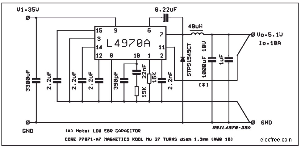
A compact and easy-to-build 5V 10A power supply circuit is sought. This circuit utilizes the L4970A IC as a 10A switching regulator. It is designed to be straightforward, serving as an example of an integrated ready-made circuit. An important...
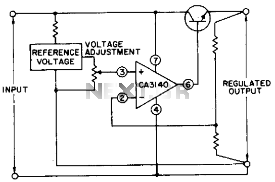
The circuit utilizes a CA3140 BiMOS operational amplifier that is capable of providing a regulated output adjustable from approximately 0 to 24 volts. The circuit is fully regulated. The CA3140 BiMOS operational amplifier is a versatile component that combines the...
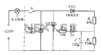
An incandescent lamp operates with a two-wire connection and features a life extension open circuit. It has a longer warm-up time compared to other types of lamps, resulting in a significant delay before illumination. Upon closing the switch, a...

The circuit is a common three-terminal linear regulator expansion flow circuit. In practical applications, it may encounter some well-considered or lower false failures. 1. Disadvantages of this power supply: 1.1 This power supply is a linear regulator...
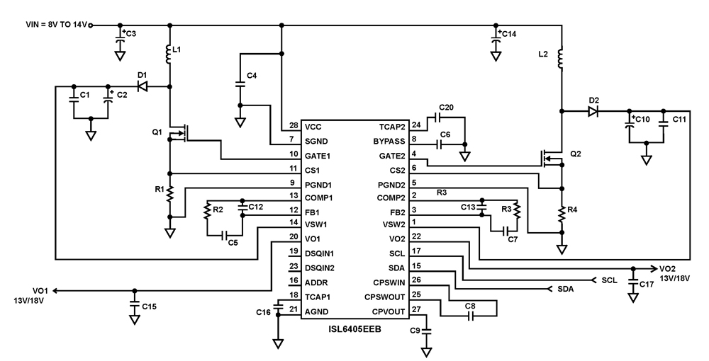
The ISL6405 is a highly integrated voltage regulator and interface integrated circuit (IC) designed to supply power and control signals from advanced satellite set-top box (STB) modules to the low noise blocks (LNBs) of two antenna ports. This device...