
Switching Voltage Regulator

The ACP3610 voltage doubler is designed for applications requiring efficient voltage conversion with minimal ripple and loss. Its architecture utilizes a dual charge pump system that alternates between charging and discharging, allowing for continuous power delivery. The design emphasizes the importance of selecting capacitors with low ESR to ensure that the voltage doubler operates within its optimal parameters. The low ESR capacitors not only enhance the efficiency of the charge pumps but also stabilize the output voltage against fluctuations caused by load changes.
The shutdown feature is particularly useful in battery-operated devices, where power conservation is critical. By controlling the enable pin, the device can be turned off when not in use, significantly reducing power consumption.
In terms of layout considerations, the placement of the input and output capacitors should be as close as possible to the IC pins to minimize inductance and resistance in the circuit. This practice will further enhance the performance of the voltage doubler by reducing voltage spikes and ensuring stable operation under varying load conditions.
For applications where higher output currents are required, multiple ACP3610 devices can be paralleled, provided that appropriate load-sharing techniques are implemented to ensure balanced current distribution among the devices. This scalability allows for flexibility in design, accommodating a wide range of output power requirements.
Overall, the ACP3610 represents a robust solution for voltage doubling applications, combining high efficiency, compact size, and ease of integration into various electronic systems.The Analog Devices ACP3610 is a voltage doubler that works with a switched-capacitor converter, using the push-pull principle. The switching frequency at the output is approximately 550 kHz. The term push-pull` refers to the two charge pumps, which work in parallel but in opposite directions in order to deliver the output voltage and current.
When ever one capacitor is supplying current to the output, the other one is being charged. This technique minimizes voltages losses and output ripple. The converter works with input voltages between 3 and 3. 6 V. It provides an output voltage of around 6V at a maximum current of 320mA, if 2. 2 µF switched capacitors with low ESR (equivalent series resistance) are used. A shut-down input is provided to allow the voltage doubler to be enabled or disabled by a logic-level signal. The IC is enclosed in a special package, which can dissipate up to 980mW at room temperature. The schematic diagram shows a typical application for the ADP3610. Here it works as a non-regulated voltage doubler. In theory, a voltage doubler can provide exactly twice the input voltage at its output, but in practice the combination of internal losses in the electronic switches and the internal resistances of the capacitors always causes the output voltage to be somewhat lower.
The output voltage drops from a no-load value of 6 V to 5. 4 V with a 320mA load, with a nearly linear characteristic. A small capacitor is connected across the two supply pins at the input of the IC. It suppresses noise, brief voltage‚uctuations, and current peaks when the ADP3610 switches. This capacitor (CIN) must have a low internal resistance (ESR). A larger capacitance value is necessary if long supply leads to the ADP3610 are present. The 1 µF output capacitor (CO) is alternately charged by the two capacitors of the charge pump, CP1 and CP2. The internal resistance is an important factor here as well. It largely determines the amount that the voltage drops under load, and the amount of ripple in the output voltage.
Ceramic or tantalum capacitors are recommended. The ESR can also be reduced by connecting several smaller-value capacitors in parallel. With small loads, the value of CO may be reduced. 🔗 External reference
Related Circuits
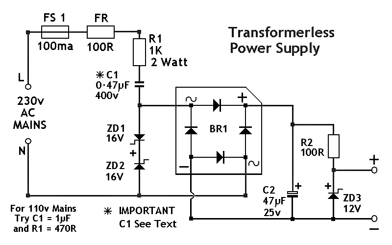
The circuit diagram was designed to create a power supply without utilizing any transformer circuit. This circuit illustrates the advantages as well as the limitations of transformerless power supplies. The transformerless power supply circuit typically employs a capacitive dropper method...
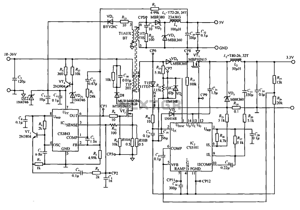
The CS3843 and CS5101 are components of a 5V/3.3V switching DC power supply circuit. The CS3843 is a fixed frequency PWM controller characterized by a set oscillator that precisely controls the duty cycle. It features a temperature-compensated reference voltage,...
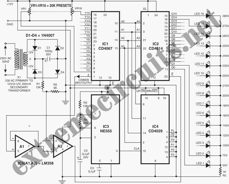
Continuous monitoring of mains voltage is essential in various applications, including manual voltage stabilizers and motor pumps. Although an analog voltmeter is cost-effective, it has several drawbacks due to its moving parts and sensitivity to vibrations. The solid-state voltmeter...
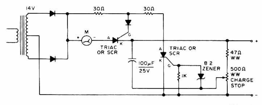
The charging circuit features adjustable voltage output settings, allowing for regulation of the charging voltage supplied to the battery. The use of a potentiometer facilitates precise voltage management, with adjustments possible down to the millivolt range. Refer to the...
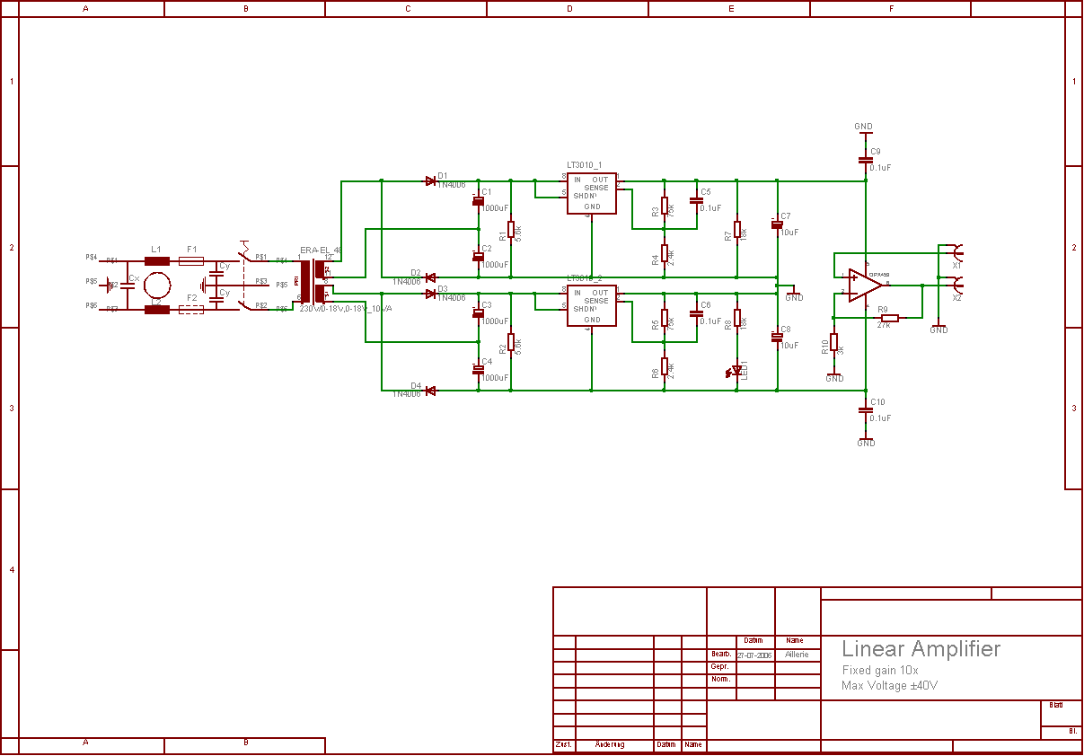
The aim of this project was to develop a linear analogue amplifier designed for laboratory use. This amplifier has to realise a voltage amplification of 10x and is intended to amplify function generator signals for tests. Power supply requirements:...
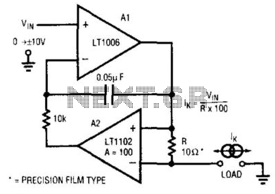
This circuit is a programmable current source that utilizes the LT1102 operational amplifier from Linear Technology Corp. in conjunction with the LT1006 operational amplifier. The first amplifier (A1), biased by a voltage source, drives current through a resistor (R)...