
Synchronized Mains Voltage Power Control

The step-down circuit is designed to reduce the input voltage level to a more manageable value for the inductive load (L1), which is critical in applications where high voltage levels could damage sensitive components. The circuit employs a combination of passive components to achieve this voltage regulation.
The turn-on delay of approximately 7 ms is a crucial feature, allowing the circuit to stabilize before the inductive load is energized. This delay is determined by the time constant formed by capacitor C2 and resistor R3, calculated as τ = R3 × C2. This time constant ensures that the capacitor charges to a sufficient voltage before the load is activated, thereby preventing inrush currents that could lead to circuit instability or component failure.
The discharge mechanism for capacitor C2 is facilitated by the diode bridge comprising diodes D1 and D2. This arrangement allows C2 to discharge rapidly at each zero voltage crossing of the line input, effectively resetting the voltage across the capacitor. Resistor R2 plays a role in limiting the discharge current, ensuring that the diodes operate within their specified current ratings while also influencing the speed of the discharge process.
The circuit's design ensures that the voltage across the load is reset with each new half line cycle, maintaining the turn-on delay consistently across cycles. This feature is particularly beneficial in applications requiring precise timing and voltage control, such as in motor control circuits or lighting systems where inductive loads are prevalent. Overall, this step-down circuit effectively balances the need for voltage reduction with the operational requirements of inductive load management.A step-down circuit used to approximately divide by two the rms voltage between the line input and the inductive load (L1) is shown on circuit diagram below. A turn-on delay of approximately 7 ms is provided by C2 and R3. We can discharge C2 at each line zero voltage using diode bridge, with diodes D1 and D2 and R2 resistor.
The voltage charge wil l be reset at each new half line cycle, and the turn-on delay will be maintained the same. 🔗 External reference
Related Circuits
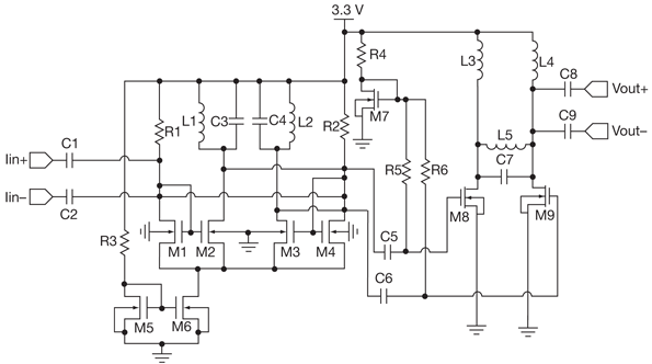
It is possible to apply switch-mode techniques to a silicon CMOS semiconductor process to create a current-mode power amplifier with high gain and efficiency for use in 2.4-GHz wireless applications. Amplification at 2.4 GHz is essential for various wireless...

AVR has two different programming modes called Parallel Programming Mode (Parallel Mode) and Serial Downloading Mode (ISP mode). In Parallel Mode, the programming is done using multiple data lines simultaneously, allowing for faster programming speeds. This mode is typically...
The following circuit illustrates a simple stepper motor controller circuit diagram. This circuit is based on the 7404 integrated circuit. Features include suitable heat dissipation. The simple stepper motor controller circuit utilizes the 7404 hex inverter IC to control the...
This voltage regulator for devices that utilize solar cells is straightforward and requires only a few electronic components. When a rechargeable energy storage device is employed, the voltage regulator circuit facilitates charging when the output voltage of the cell...
The rectifier input is connected to the input, establishing a relationship where gain is inversely proportional to the input level. Consequently, a 20-dB reduction in input level results in a 20-dB increase in gain. The output is designed to...

The circuit is a two-stage, direct-coupled transistor amplifier configured as a free-running multivibrator. Both the flash duration and flash interval can be adjusted by turning the potentiometer, R1. The described circuit operates as a two-stage, direct-coupled transistor amplifier, functioning as...