
Test Transmitter

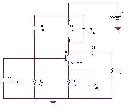
The Hall Effect switch comprises resistors and capacitors, including R1, C1, U1, U2, and C2 (see S3020_1). Component U1 is an A1171 Hall Effect sensor with a quiescent consumption of a few microamps. It activates for 80 microseconds out of every 60 milliseconds, corresponding to a switching frequency of approximately 18 Hz. With R1 set to 50 kΩ and C1 to 4.7 µF, a 100 mV linear drop is observed at U1-6 during the active phase, indicating a current of 5.9 mA from C1. After the active period, the voltage at U1-6 rises with a time constant around 30 milliseconds, consistent with the RC time constant of 50 kΩ and 4.7 µF, which equals 24 ms. The average voltage drop across R1 is measured at 280 mV with a 10 MΩ, G=10 probe, indicating an average current of 5.6 µA. A digital voltmeter (DVM) measures 5.3 µA after accounting for a 0.2 µA offset. When using a 1 MΩ, G=1 probe, a 420 mV drop occurs due to the probe's current draw, resulting in a total of 8.4 µA. Notably, the current measured by the DVM increases to 5.6 µA when R1 is touched with the G=10 probe. The voltage on VBAT shows a 0.5 mV drop over 5 ms, synchronized with U1's active period, followed by a rise of 0.5 mV over 55 ms. Initially, R1 was set to 1 kΩ, but this value led to a 50 mV noise on VBAT due to current surges through U1. Increasing R1 to 50 kΩ resulted in unreliable activation of U1 upon power connection, causing it to draw 40 µA with approximately 1.5 V across R1. A short across R1 using tweezers was necessary to initiate normal operation. When a magnet approaches U1, it triggers U2, a D-type flip-flop. The output from U1 (U1-1) toggles between low (0 V) and high (VBAT), serving as the power source for the entire transmitter circuit, which is decoupled with C2, a 4.7 µF capacitor. The internal switching frequency of U1 at 18 Hz may introduce noise into the transmitter amplifiers, but with proper functioning of C1 and R1, the amplitude of this noise at the input remains below 5 µA.The Test Transmitter (A3020) is a combination of three circuits. Its purpose is to allow us to test the Subcutaneous Transmitter ( A3019 ) and to investigate SAW (surface acoustic wave) VCOs (voltage-controlled oscillators). The A3020 contains the complete A3019 circuit in its center section. The circuit is almost identical to that of the Subcutan eous Transmitter ( A3013 ). The most significant changes are as follows. Replace reed switch with Hall Effect Switch. The old magnetic switch was easy to break and large, not to mention its being discontinued by the manufacturer. Magnet turns off all power to circuit except Hall Effect Switch. The transmitter is either ON or OFF. When it`s OFF, the only current drain is the Hall Effect Switch. When it is ON, it is transmitting. Two op-amps used for amplification and filtering instead of three. We reduce the DC gain of the main amplifier stage by adding a capacitor to its feeback loop. The capacitor sets the lower limit of the operating bandwidth at around 1 Hz. Power supply decoupling done so as to favor analog circuits. We use the battery and regulator directly for analog circuits, and supply current to the digital circuits and VCO through resistors that keep transmission noise off the analog supplies.
The SAW VCO circuits continue the earlier work we did with our RF Tester ( A3014 ) and RF Combo ( A3016 ) circuits. In the new SAW circuits, we are able to vary the feedback track length in order to provoke oscillations, and we are able to short a stub track to ground in order to cause phase changes.
Figure: The A3020A Circuit. The middle section provides the circuit drawn in S3020_1, the test transmitter. The right section, which we have cut off because it is independent, provides S3020_2, the SAW oscillator. The left section uses signals from the logic chip in the test transmitter, and provides S3020_3. [26-FEB-10] The Hall Effect Switch consists of R1, C1, U1, U2, and C2 (see S3020_1 ). Component U1 is a A1171 Hall Effect sensor. Its quiescent consumption is a few microamps. It turns on for 80 s out of every 60 ms (roughly 18 Hz switching). With R1 = 50 k © and C1 = 4. 7 F, we see a 100-mV linear drop on at U1-6 during the active period, or 1. 2 V/ms, which indicates 5. 9 mA out of C1. After the active period, the voltage on U1-6 rises with a time constant of around 30 ms, which is consistent with RC = 50 k © G— 4.
7 F = 24 ms. The average voltage drop across R1, meanwhile, is 280 mV when measured with a 10-M ©, G—10 probe, indicating an average current of 5. 6 A. Our DVM measures 5. 3 A (after subtracting 0. 2- A offset). If we use a 1-M ©, G—1 probe to measure the voltage drop, we see 420-mV drop because of current drawn by the probe, bringing the total to 8.
4 A. The current measured by our DVM increases to 5. 6 A when we touch R1 with the G—10 probe. On VBAT, we see a 0. 5-mV drop over 5 ms synchronous with the active period of U1. After that, VBAT rises 0. 5 mV over 55 ms. At first, we had R1 = 1 k ©, but with this smaller value we saw 50-mV of noise on VBAT as a result of the current surges through U1. We increased R1 to 50 k ©. But we now find that U1 does not turn on reliably when we connect power. It will get stuck consuming 40 A, with roughly 1. 5 V across R1. We must short R1 with tweezers to get the chip to start up, after which it runs normally. When we move a magnet near U1, it turns clocks U2, which is a D-type flip flop. The output of U1, which is U1-1, toggles between LO, or 0V, and HI, or VBAT. We use U1-1 as our source of power for the entire transmitter circuit, and decouple it with C2, a 4. 7 F capacitor. The 18-Hz internal switching frequency of U1 is a potential source of 18-Hz noise in the transmitter amplifiers.
With C1 and R1 functioning correctly, the amplitude of this noise at the input is less than 5 A. Table: Subcutaneous Transmitter Current Consumption. In each case we allow the circuit to 🔗 External reference
Related Circuits
A simulation of a 27 MHz transmitter circuit is to be conducted using PSPICE. The circuit diagram is provided as Figure 1 in the following content. The 27 MHz transmitter circuit typically consists of several key components, including an oscillator,...
If the audio input is a microphone, it is expected to precede an amplifier to achieve an output power of approximately 8W. The amateur seeking to enhance a small transmitter, which is likely already constructed, can utilize this circuit,...
Field-effect transistors (FETs) are integral components found in various applications such as power sections, LCD inverters, uninterruptible power supplies (UPS), amplifiers, monitor B+ circuits, and ATX power supplies. When a FET fails, it is essential to use a meter...
The following diagram is the schematic diagram of a four-transistor FM transmitter circuit designed by Paul K. Sherby. Components List: R1, R2, R8 = 1K, R3 = 100K, R4 = 150K, R5, R7 = 10K, R6 = 220 ohm,...
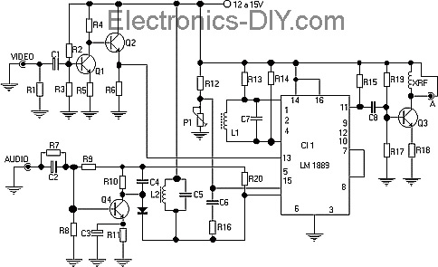
This TV transmitter transmits audio and video signals from camcorders, DVD players, VHS players, satellite systems, video games, etc., broadcasting them on a channel free from the VHF strip. These signals can be radiated using a common antenna and...
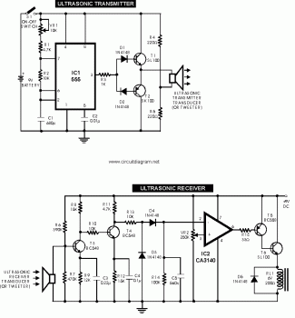
This circuit explains alternate wireless switching using an ultrasonic sensor. The distance of the switching range should be more than 10 meters. The described circuit employs an ultrasonic sensor to facilitate wireless switching, allowing for the activation or deactivation of...