
The KD2BD ATV AM Video Modulator

When the Brookdale ATV Repeater System was first constructed, a PC Electronics model RTX-70 exciter was used in the transmitter portion of the repeater. However, the intermodulation distortion products generated by the exciter when amplified by a Mirage D100ATV-R amplifier were so severe, they completely overwhelmed the repeater's receiver, despite the extensive combline and interdigital filtering used in the system.
After much study and research, the cause of the exciter's strong IMD products was found to be the result of distortion and non-linearity in the exciter's video modulator, and not the modulated RF stages themselves. Once the original video modulator was replaced with the one described on this page, the harmful effects of IMD were reduced to imperceptible levels. An added bonus was a noticeable increase in the exciter's RF power output. This method of sync expansion is unique in that it also compensates for audio subcarrier compression at sync time, resulting in a clean output signal with no sync buzz in the transmitted audio. The first section of the video modulator performs a video level clamping function. The high input impedance Darlington amplifier and the small series coupling capacitor combine to achieve an excellent low-frequency response and a clamping function with very rapid response time. A three terminal voltage regulator sets the clamping level to 8 volts. The clamped video is then level shifted through a zener diode and applied to a single video amplifier stage. A PNP transistor in the collector circuit functions as a constant current source for the video amplifier. The use of a constant current source rather than a collector load resistor in the video amplifier results in very high voltage gain with nearly rail-to-rail output voltage capability. Negative feedback around the video amplifier reduces the gain to the amount required, while it increases the bandwidth, flattens the frequency response, increases the linearity, and reduces any distortion products to extremely low levels.
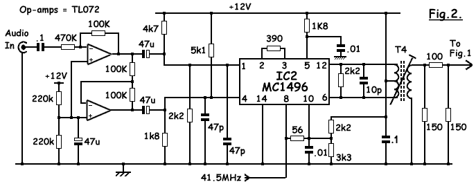
The described circuit utilizes a 2N3904 transistor to establish the quiescent point (Q point) for the amplifier, which is crucial for linear amplification. The inclusion of a 3300-ohm resistor and a DC blocking capacitor allows for the integration of FM subcarrier audio at 4.5 MHz into the base circuit, ensuring that the audio signal is properly coupled without DC offset affecting subsequent stages. The RF power stage employs a 2SC1909 transistor, noted for its capability to handle high frequencies and power levels, making it suitable for the final amplification stage of the modulator.
In addition, the circuit includes an LM311 voltage comparator that processes clamped video signals for sync detection. The option to use an LM1881 sync separator chip provides flexibility in design, catering to varying builder preferences. The output sync pulses trigger a CD4016B silicon bilateral switch, which dynamically adjusts the negative feedback around the video amplifier. This adjustment is critical during sync periods, as it mitigates the effects of gain compression that may occur in linear power amplifiers following the video modulated stages.
The design of the video modulator emphasizes the importance of maintaining a clean output spectrum, particularly in the context of an ATV repeater system. The original use of a PC Electronics RTX-70 exciter highlighted the challenges posed by intermodulation distortion (IMD), which can severely impact system performance. By replacing the initial video modulator with a more efficient design, significant improvements in both RF output and reduction of IMD were achieved.
The implementation of a high input impedance Darlington amplifier combined with a fast-acting clamping capacitor allows for rapid response to video signals, ensuring that the signal integrity is preserved. The voltage regulator, set to 8 volts, establishes a stable clamping level, while the subsequent level shifting through a zener diode prepares the signal for amplification.
The video amplifier stage benefits from a constant current source configuration, enhancing voltage gain and enabling nearly rail-to-rail output. This approach, coupled with negative feedback, optimizes performance by broadening bandwidth, improving frequency response, and minimizing distortion, thus ensuring high fidelity in the transmitted video signal.A 2N3904 in the base circuit sets the `Q' point of the amplifier. FM subcarrier audio at 4.5 MHz is also injected at this point through a 3300 ohm resistor and a DC blocking capacitor. A high frequency 5-watt RF power transistor (2SC1909) serves as the last stage of the modulator. An NTE-235, NTE-236, or equivalent is suitable in this application. Clamped video is also fed into an LM311 voltage comparator that serves as a video sync detector. Some builders have used an LM1881 sync separator chip for this stage. Either way, sync pulses detected by this circuit trigger a CD4016B silicon bilateral switch that lowers the negative feedback around the video amplifier and voltage follower at sync time to compensate for high power gain compression in any solid-state linear power amplifiers that may follow the video modulated stages.
Building an in-band, duplexed ATV repeater system is not a trivial task. Just ask anyone who's tried. The output spectrum of the repeater's transmitter must be extremely clean, and both the transmitter's output as well as the receiver's input must be tightly filtered to achieve adequate isolation and reject interference from strong signals on neighboring frequencies. When the Brookdale ATV Repeater System was first constructed, a PC Electronics model RTX-70 exciter was used in the transmitter portion of the repeater.
However, the intermodulation distortion products generated by the exciter when amplified by a Mirage D100ATV-R amplifier were so severe, they completely overwhelmed the repeater's receiver, despite the extensive combline and interdigital filtering used in the system. After much study and research, the cause of the exciter's strong IMD products was found to be the result of distortion and non-linearity in the exciter's video modulator, and not the modulated RF stages themselves.
Once the original video modulator was replaced with the one described on this page, the harmful effects of IMD were reduced to imperceptible levels. An added bonus was a noticeable increase in the exciter's RF power output. This method of sync expansion is unique in that it also compensates for audio subcarrier compression at sync time, resulting in a clean output signal with no sync buzz in the transmitted audio.
The first section of the video modulator performs a video level clamping function. The high input impedance Darlington amplifier and the small series coupling capacitor combine to achieve an excellent low-frequency response and a clamping function with very rapid response time. A three terminal voltage regulator sets the clamping level to 8 volts. The clamped video is then level shifted through a zener diode and applied to a single video amplifier stage.
A PNP transistor in the collector circuit functions as a constant current source for the video amplifier. The use of a constant current source rather than a collector load resistor in the video amplifier results in very high voltage gain with nearly rail-to-rail output voltage capability.
Negative feedback around the video amplifier reduces the gain to the amount required, while it increases the bandwidth, flattens the frequency response, increases the linearity, and reduces any distortion products to extremely low levels. 🔗 External reference
Related Circuits
With the impending shutdown of the 405-line transmitter network, individuals with collections of early television sets must find new methods to supply them with appropriate signals. Regardless of the scheme implemented, a method for converting baseband audio and video...

Two integrated circuit (IC) RF modulators are utilized to convert a suitable baseband video and audio signal into a low VHF modulated carrier, specifically channels 2 through 6 in the U.S. and channels 1 through 3 in Japan. The...

The LT6552 is a video difference amplifier optimized for low voltage single supply operation. The LT6552 features a 75MHz 3dB bandwidth, a 600V/µs slew rate, and ±70mA output current, making it ideal for driving cables directly. This circuit maps...
This varactorless high-frequency modulator electronic project must be powered by a simple DC 3-volt power source, such as a 3-volt battery. Traditionally, high-frequency oscillators are frequency-modulated using a varactor. However, varactors typically require a significant voltage change to achieve...
This is a simple video transmitter capable of transmitting signals up to 50 meters. It can be connected to a camera or other video sources, allowing viewing on a VHF channel analog TV. The transmitter operates on a supply...
The circuit schematic of the UDC consists solely of dispersive components. Two low-frequency series LC resonators, with equal inductances (LA=LB) and capacitances (CA=CB), are connected to two input semi-infinite transmission lines, designated as A and B. These resonators are...