
Thermocouple amplifier gain circuit

The OP07 operational amplifier is designed for precision applications requiring minimal drift and noise, making it suitable for instrumentation and industrial sensor applications. Its low voltage drift and noise specifications ensure that the output remains stable over temperature variations and extended periods, which is critical in environments where accuracy is paramount.
In the differential instrumentation amplifier configuration, the resistors R3 and R1 play a vital role in setting the gain of the amplifier, allowing for fine-tuning of the output based on the specific application requirements. The ability to convert voltage signals into a standard current output (4-20 mA) is particularly beneficial in industrial settings where current loops are commonly used for signal transmission over long distances, minimizing the effects of noise and interference.
The circuit's performance can be further enhanced by selecting precision resistors for R1, R2, R3, and R4, which will help maintain the desired gain accuracy and linearity. Additionally, the choice of the reference voltage source is crucial for ensuring that the output current is consistently within the desired range, particularly under varying load conditions.
Overall, the OP07 operational amplifier, with its low drift, low noise, and flexible configuration options, serves as a robust solution for high-performance analog signal processing tasks in various electronic applications.OP07 low drift (maximum voltage drift 30 FLV, maximum drift 0.6vV / aC), low noise (maximum 0.6 pLVp.P), ultra-stability (maximum 0.6yV / qC. Months), wide supply voltage range (t3 ~ + 18V), high-performance operational amplifiers. OP27 and OP07 closer parameters (see table). Their pin functions shown in Figure LO-l, the application circuit as shown in FIG. When R3: R4, Ri = R2 when, OP07 constitute a differential instrumentation amplifier, the amplifier gain is determined by R3 / RI. Figure 10-2, Figure 10-3 are two cases of common operation amplifier circuit, the circuit configuration of the operational amplifier and the general structure of the same.
The circuit can be amplified input signal of the sensor is converted to 4 ~ 20mA current output circuit mainly by the operational amplifier, a reference voltage source, the output tubes. Input voltage through the operational amplifier, V driven by the sampling resistor R6 , the load resistance Ri.
In the form of a current output. Output current and input voltage relationship between the / ou-r = (VIN Rs / Rz + 5Rs / R,) / R6 according to the figure parameter / ourr = (16VlN / JOO) + 4.O (mA)
Related Circuits
Over-Temperature Alarm Circuit Uses Common, Inexpensive Components | Negative-temperature-coefficient (NTC) thermistor, ICs. The Over-Temperature Alarm Circuit is designed to detect excessive temperatures and provide an alert using readily available and cost-effective components. The core sensing element of this circuit is...
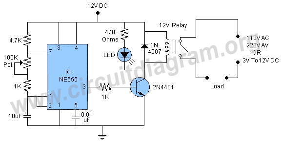
The circuit operates continuously, turning on and off. It utilizes the widely recognized NE555 timer IC, known for its versatility in various electronic applications. In this configuration, the IC is set up as an astable multivibrator. A 12-volt relay...
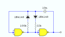
A simple square wave oscillator can be created using two gates from a CMOS 4011 NAND chip. Alternatively, a CMOS 4001 chip or a TTL equivalent can also be utilized. In this circuit, the mark-space ratio can be independently...
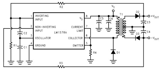
This RS232 power supply circuit diagram is a simple RS-232 line driver power supply that operates from an input voltage as low as 4.2V and delivers an output of ±12V at ±40 mA with an efficiency of better than...
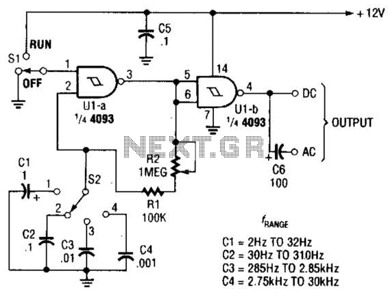
The circuit illustrated operates within a frequency range of 2 Hz to 30 kHz. Additionally, R2 is configured as either a linear or logarithmic potentiometer. The circuit is designed to accommodate a wide frequency spectrum, making it suitable for various...
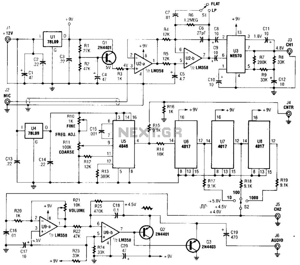
The precision audio frequency generator consists of several sub-circuits: an audio amplifier/filter circuit, an automatic level control, a variable voltage-controlled oscillator, a frequency divider circuit, an integrator, and an audio output amplifier. An electret microphone element is utilized to...