
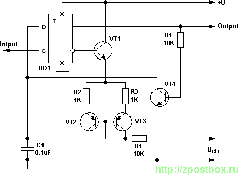
Thrifty Voltage Regulator

The described voltage regulator circuit utilizes a series configuration with transistor T1 to efficiently regulate the output voltage while minimizing power loss. The design allows for operation with a lower input voltage, making it suitable for battery-powered applications. The inclusion of a variable reference voltage source created by diodes D1-D3 or a zener diode (D4), along with resistors R5 and potentiometer P1, facilitates fine-tuning of the output voltage. This adaptability is crucial in applications where precise voltage levels are required.
Transistor T3 plays a vital role in monitoring the output voltage. When the output falls below the set threshold, T3's base potential decreases, leading to a reduction in its conduction. This change raises the collector voltage, which in turn increases the base voltage of T2, enhancing the drive to T1. This feedback mechanism ensures rapid restoration of the output voltage, demonstrating the circuit's responsiveness to variations in load or input voltage.
The BATT-LOW indicator circuit is an essential feature, providing a visual cue when the battery voltage approaches a critical level. The design options for this indicator allow for flexibility in implementation, whether through a standard LED or a more sophisticated liquid-crystal display. The careful selection of resistor values, particularly R7b, is crucial to protect sensitive components within the circuit from potential damage due to excessive current.
Overall, this voltage regulator circuit is characterized by its low quiescent current draw, effective voltage regulation capabilities, and the ability to operate efficiently with a decreasing battery voltage, making it an excellent choice for portable electronic devices.One of the drawbacks of a three-pin voltage regulator is that the input voltage needs to be 2. 5 3 V higher than the output voltage. This makes these integrated regulators unsuitable for battery power supplies. If, for instance, the output voltage is 5 V, a 9 V battery could be discharged to 7. 5 V or thereabouts only. On top of this, most of thes e regulators draw a current of about 2 mA. Special low-drop versions sometimes offer a solution, but they are not ideal either. The regulator described here is rather thriftier: it draws a current of only 300 µA and the difference between its input and output is only 100 200 mV In the circuit diagram, T1 is arranged as a series regulator, which means that the difference between input voltage and output voltage is limited to the transistor`s saturation potential. Therefore, a 9 V battery can be discharged to about 5 V, which is quite an improvement on the situation with an integrated regulator.
Diodes D1-D2-D3, or a suitable zener diode (D4), in conjunction with R5 and P1, form a variable reference voltage source, which is used as the (output-dependent) base potential of T3. If the output voltage drops below a desired level, the base potential of T3 also drops. The transistor then conducts less hard and its collector voltage rises. The base voltage of T2 also rises, so that T1 is driven harder. This results in the near-instantaneous restoration of the output voltage. The design of the reference voltage source is clearly of paramount importance. The current through the LEDs or the zener diode is of the order of only 100 µA. This means that thedrop across a 5. 1 V zener diode is only 4. 3 V and across each LED, only about 1. 43 V. For a wanted output voltage of 4. 8 V, the three LEDs proved very effective, whereas the zener did not. It may well be necessary, if a zener diode is used, to try one rated at 4. 7 V. If, however, an output voltage of 5 V is wanted, it will be necessary to carefully select a zener diode.
When the battery voltage has dropped to a level where it is only marginally higher than the wanted output voltage, T1 and T2 conduct hard. A further drop in the battery voltage will cause the collector potential of T2 to drop rapidly to 0 V, since T2 tries to make T1 conduct hard.
The large drop in the collector potential of T2 may be used to drive a BATT-LOW indicator. This may be done in three ways as shown in Figure 2. When network a is connected between terminals A and B, transistor T4 will normally be held cut off by divider R6-R7a. If then the voltage at B drops suddenly, T4 conducts, where-upon D5 indicates that the battery is nearly flat.
The network in b is similar to that in a, but is intended for a liquid-crystal display of BATT-LOW. The collector of T4 is linked to the IC that drives the decimal point and the BAT-LOW segment of the display. Network c may be used if there is an unused inverter or gate in the circuit to be powered. The high value of resistor R7b prevents the internal protection diodes of the IC being damaged. When the regulator has been built, connect it to a variable power supply via a multimeter set to the mA range and set P1 roughly at its mid-position.
Turn P1 slowly until the desired output voltage is obtained. If with an output voltage of 4. 8 V the regulator draws a current of more than 250 300 µA, the three LEDs or zener diode must be replaced. The regulator can provide a current of up to about 25 mA. With a fresh 9 V battery, the dissipation of T1 does not exceed 100 mW. If the input voltage is higher, it may be necessary to mount the transistor on a suitable heat sink or replace it by a power transistor, for instance, a Type BD138.
🔗 External reference
Related Circuits
This voltage-controlled frequency divider circuit produces lower frequency pulses that depend on the control voltage, with synchronous rising edges for the input and output pulses. Typically, such frequency dividers utilize a monostable circuit connected between an inverted output and...
This simple reference circuit provides a stable voltage reference that is nearly free from supply voltage noise. Typical power supply rejection exceeds 100 dB. The described voltage reference circuit is designed to deliver a consistent output voltage while minimizing the...

This is a simple design for a voltage regulator circuit using a pass transistor. The design is built around the LM317T. The output current of the LM317T can be increased by incorporating an additional power transistor to share a...

This is a 5V to 12V DC-DC step-up (boost) converter circuit designed specifically for USB-powered applications. A USB port has two current supply modes. Initially, it supplies a maximum of 100mA to the load before detecting the connected device....
This circuit offers a distinctive solution to a prevalent power distribution issue at the system level. When the supply voltage to a remote board must travel through a lengthy cable, the voltage at the termination point may decrease to...

This circuit is connected to a motorcycle and is integrated into a circuit that is powered only when the key is in the "ON" position. If the motorcycle is turned off using the kill switch while the key remains...