
Time Delay Switch with Triac

The time delay switch circuit operates on the principle of controlled timing and voltage management to provide a safe and reliable method for activating AC loads. The circuit begins with the connection to the AC mains, where the resistor R1 is employed to limit the voltage to a manageable level for the subsequent components. The rectification of the AC voltage is performed by diode D1, which converts the alternating current to direct current, suitable for charging capacitors.
The capacitor C1 plays a critical role in the timing mechanism of the circuit. Its high capacitance value ensures that it takes a sufficient amount of time to charge, thus creating the desired delay before the SCR is triggered. The SCR (Silicon Controlled Rectifier) is a semiconductor device that acts as a switch, allowing current to flow only when it receives a gate pulse. The timing of this pulse is contingent upon the complete charging of C1, which is designed to take approximately two minutes.
Upon reaching the required charge, the SCR is activated, allowing current to flow to capacitor C2. This additional capacitor serves to prolong the delay before the TRIAC is triggered, providing an extra minute before the AC load is energized. Resistor R3 is crucial in this stage as it facilitates the gate triggering of the TRIAC, ensuring that the load receives power only after the complete time delay has elapsed.
The TRIAC, once triggered, allows current to pass through to the connected AC load, effectively turning it on. Capacitor C3 is included in the design to stabilize the gate voltage of the TRIAC, preventing any unintended turn-off due to voltage fluctuations or back EMF from the load.
Safety measures are paramount when working with this circuit due to its connection to high voltage AC mains. Adequate precautions must be taken to avoid electric shock, and it is strongly recommended that the assembly and testing of this circuit be performed by qualified personnel with experience in handling high-voltage electronics.This time delay switch circuit is useful to switch on an AC load such as lamps after the delay of three minutes. This protects the load from inrush current and transients at power on which may be detrimental to the device.
The time delay switch is directly connected to the AC lines to derive power to the components. Resistor R1 drops AC voltage an d D1 rectifies the same to give low volt DC. The high value capacitor C1 act as a smoothing capacitor as well as the time delay device. That is the SCR conducts only after C1 is fully charged. It takes around 2 minutes. When C1 charges fully gate of SCR gets firing pulse and it conducts. This charges C2 which also give another one minute to fire the Triac trough R3. When the triac conducts, AC load gets electrical continuity and turns on. Capacitor C3 keeps the voltage level at the gate of triac and eliminates the back lash effect. Note:Take extreme care while handling the circuit, since it is at mains lethal potential. Do not touch any points when it is connected to mains. It should be constructed only by an experienced person. 🔗 External reference
Related Circuits
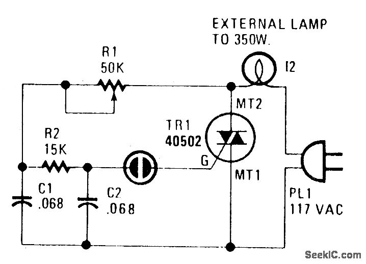
A heatsink allows the TRIAC (TR1) to manage power levels up to 350 watts. The neon lamp (I1) will not activate the gate until it is in conduction, and resistor R1 is used to adjust the lighting level as...
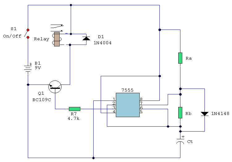
The following circuit illustrates a timer circuit with independent mark and space periods. It is based on the 7555 integrated circuit (IC). The high output duration is calculated by T(on) = 0.7 Ra Ct, while the low output duration...

Some time ago, an electronic hobbyist sought to create a logic analyzer. As a DIY enthusiast, a simple yet effective logic analyzer was constructed. Utilizing an old Pentium III laptop equipped with a single LPT port, a search for...
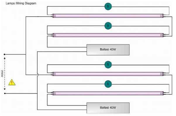
Four blacklight lamps, 15W each, emit radiation in the UVA region, with a peak around 350nm where the thin surface above the copper of the photosensitive board is sensitive. The lamps are taken by two and are connected in...
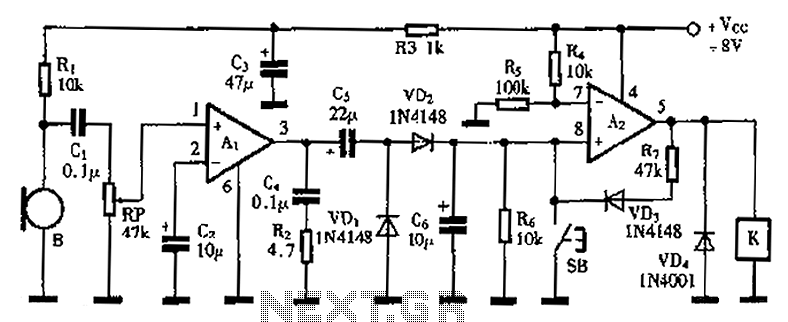
A practical voice-activated switch is presented. An A1 amplifier is connected to a conventional microphone (B) that picks up the audio control signal, which is then amplified. After amplification, the signal passes through components C5, VD1, and VD2, forming...
This entry is for the international 555 Contest. The 555 timer chip has been in use for many years and is highly versatile. The concept of this project addresses the need for notification of an event while away from...