
TNT1541 diy zero-oversampling dac

The TNT Convertus DAC design showcases innovative engineering principles in digital-to-analog conversion. The use of the TL431 voltage reference as a shunt regulator enhances power supply stability and performance, which is crucial for audio applications. The implementation of multiple digital inputs allows for flexibility and adaptability, catering to various user needs and preferences. The choice of using a ferrite toroid transformer for signal decoupling underscores the importance of minimizing electromagnetic interference, ensuring that the digital signals remain intact and free from noise. The design's consideration for both RCA and BNC connectors reflects a thoughtful approach to compatibility and signal integrity, allowing users to select the best option for their setup.
In summary, the TNT Convertus DAC represents a significant contribution to the DIY audio community, combining practical design elements with advanced engineering techniques to deliver high-quality audio performance. Its thoughtful design choices, from power supply regulation to input flexibility, make it a valuable project for enthusiasts looking to explore the world of digital audio conversion.The TNT Convertus has been one of my favorite designs. It was probably one of the first DAC DIY projects published in Italy, and attracted a lot of attention (well, given the size of the market, obviously. ). A few changes have been made to the original Convertus design, but I never had the time to test another DAC: it would have required a complet
e overhaul of the project, including a new PSU. Anyway, rumours about the outstanding quality of another DAC chip have loudly continued - the DAC in question, the TDA1541A, has a slight problem: it is no longer in production. As I wanted to present an easy to build DAC, this was a condition I was not willing to accept, but after building it, I realized that the design includes a few interesting elements that can be applied to any other dac type.
Even though the DAC is now rather difficult to find, especially in the selected versions, it is still available, and in the end the situation is no worse than that of a few well known NOS tubes. One more note. I will not go back in detail over all the circuitry I have already described in the Convertus, Convertus decima and Convertus Decima Digital articles.
Please read them through before reading the present one. For the receiver I used a CS8412. At the time I`m writing this article it is still present in the RS catalogue in a DIL package. The CS8414, the current generation, seems to work a little better, but is not available in DIL format: if you dare working with a surface mount chip, it can be a valid pin to pin substitute. In order to be able to select any output configuration, the mode pins are controlled by a quadruple microswitch.
this lets me select any possible output configuration with ease. Mode 3 is to be used (M0=1, M1=1, M2=0, M3=0), unless you do not wish to implement the digital decimation circuit. In that case, you must select mode 1 (I2S compatible, all signals output). As you see, there is wide use of local regulation. A large number of TL431s are used on the different boards to decouple all power supplies. This is a precision, programmable, low cost voltage reference that is used (in this application) as shunt voltage regulator.
In this configuration it has a dynamic output impedance of 0. 1ohm up to 100KHz. Not a very original idea, anyway: I think there are at least two other DAC projects available on the net using the same feature in exactly the same position. More interesting are the digital inputs. In fact, two inputs are shown on the schematic, but you can add as many as you want, provided that you check the power supply regulation is up to the job.
Each input connection is completely de-coupled using a high frequency transformer. I used a ferrite toroid from RS Components as a core, part number 212-0831, and just wound up both primary and secondary coils with five turns of insulated copper solid core wire (the one used for normal power transformers secondary coils). Unfortunately the original ferrite toroid is no longer available; try finding something similar of small dimensions.
The digital input socket can be either RCA or BNC. I always use BNC, which can specified for a precise 75ohm impedance, but this sometimes creates problems (or requires an adapter to be used. ). In either case they must be female sockets, insulated from the panel. The digital input signal comes out of the secondary of the transformer and is taken to a digital receiver, a DS34C86.
This chip contains two differential line receivers and two drivers. The drivers have no use for us, at least for the moment. The receivers work according to the RS-422 electrical standard, which is very similar to S/PDIF electrical standard. A very interesting aspect of the chip is that the receiver has a three-state output: this means that its output can be disabled, and in this situation presents a very high impedance.
The technique is obviously used in buses, where more than one device can get con 🔗 External reference
Related Circuits
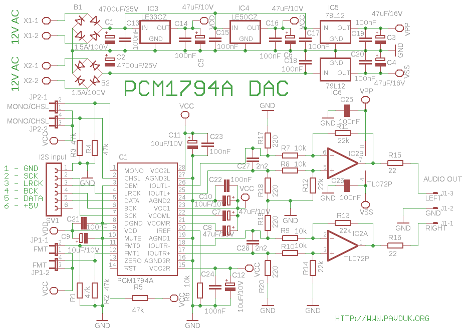
A transformer with two separate 12V secondary windings is required for the power supply. If the transformer does not have a third separate winding, the supply input of the S/PDIF decoder must be connected in parallel to the positive...
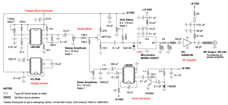
A DIY GSM jammer schematic diagram designed to disrupt cellular mobile phone signals operating within the GSM1900 frequency range of 1930 MHz to 1990 MHz. The GSM1900 standard is utilized in the USA, Canada, and most countries in South...
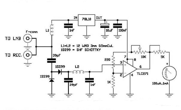
A circuit has been identified that integrates a voltage regulator and filter to isolate the voltage supplied by the receiver for powering an operational amplifier (op-amp) that drives a meter. Additionally, the circuit isolates the carrier frequency from the...
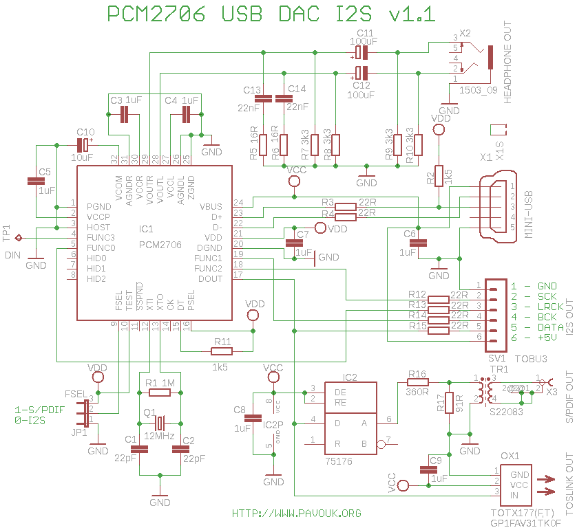
This project involves a couple of USB Digital-to-Analog Converters (DACs) that lack I2S output. Some users do not require S/PDIF input and prefer a direct USB connection. Therefore, it is unnecessary to convert the signal from USB to S/PDIF...

There is information not included in this main post. Read through the thread for more information on timer calibration and other useful information by cpfers. PEU pointed out that the TX should be connected to serial port pin 2...
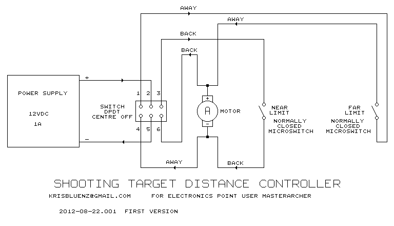
The motor is rated at 6W, which corresponds to a current of 0.5 amps at a voltage of 12V. It is recommended to use a 12V DC power supply with a rating of 1A or higher. Any type of...