
Tone-control audio amplifier

The circuit design leverages the capabilities of the CA3140 BiMOS operational amplifier, which is known for its superior performance in terms of speed and bandwidth. The high slew rate allows for rapid changes in output voltage, making it suitable for applications requiring fast signal processing. The wide bandwidth ensures that the amplifier can handle a broad range of frequencies without significant attenuation, which is critical in high-fidelity audio applications or RF signal processing.
The high input impedance characteristic of the CA3140 minimizes loading effects on the preceding stage, allowing for accurate signal representation without distortion. This feature is particularly beneficial in sensor applications where the source impedance may be high. The output voltage capability of the amplifier ensures that it can drive loads effectively, providing versatility in various circuit configurations.
With a designed gain of eleven, the circuit provides a significant amplification factor, which is essential for applications requiring a strong output signal. The gain is calculated as the ultimate boost or cut plus one, where a 20-dB boost corresponds to a voltage gain of approximately 10, leading to a total gain of eleven when considering the input signal.
In terms of input loading, the resistance from terminal 3 to ground plays a crucial role. For a 20-dB boost or cut, the input loading is effectively determined by this resistance, ensuring that the circuit maintains stability and performance under varying load conditions. This aspect is vital for preserving the integrity of the input signal and ensuring that the amplifier operates within its optimal range.
Overall, this circuit exemplifies the effective application of the CA3140 BiMOS op amp's features, providing a robust solution for signal amplification with minimal distortion and high fidelity.The circuit makes excellent use of the high slew rate, wide bandwidth, high input impedance, and high-output voltage capability of the CA3140 BiMOS op amp. The wideband gain of this circuit is equal to the ultimate boost or cut plus one, in this case a gain of eleven.
For 20-dB boost or cut, input loading is essentially equal to the resistance from terminal 3 to ground.
Related Circuits
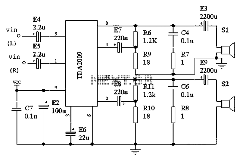
The intention was to develop a morning exercise machine, but the challenge was the absence of a suitable high-power amplifier. Since the exercise machine operates on battery power, the search for a solution persisted for several months. Eventually, the...
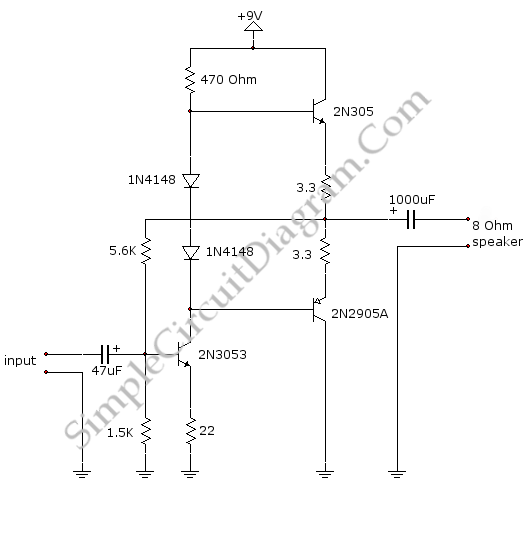
This is a small audio amplifier, similar to those used in small transistor radios. The circuit draws approximately 30 milliamps from a 9-volt supply and consists of two stages. The first stage is the input stage using a 2N3053...
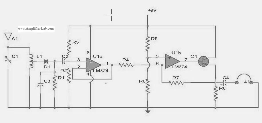
The following circuit illustrates a power amplifier electronic circuit, specifically a tube audio RF amplifier circuit diagram. This circuit is based on the LM324 integrated circuit. The power amplifier circuit utilizing the LM324 operational amplifier is designed to enhance audio...
The objective of this project was to design a compact, portable mixer powered by a 9V PP3 battery while maintaining high-quality performance. The mixer consists of three primary modules that can be adjusted in number and configuration to meet...

A schematic of the ability accumulation is presented below. Similar to the amplifier schematic, the ability accumulation design is © OddWatt Audio, and permission to host the schematic on this platform has been granted by OddWatt Audio. The schematic...
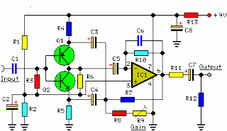
Parts List The circuit consists of a preamplifier, tone controls, and a regulated DC power supply, providing a power output of 18 Watts for an 8 Ohm load. The circuit design includes three main components: a preamplifier, tone control circuitry,...