
Transistor Circuit Analysis

The described circuit utilizes a bipolar junction transistor (BJT) configured in saturation mode, which is commonly used in switching applications. In this configuration, the transistor is fully turned on, allowing maximum current flow from the collector to the emitter. The emitter voltage of approximately 2.7 V suggests that the transistor is indeed in saturation, as this value is consistent with typical V_BE (base-emitter voltage) values for silicon transistors.
To analyze the circuit further, key parameters such as the collector current (I_C), base current (I_B), and load resistance (R_L) should be considered. The relationship between these currents can be expressed using the transistor's current gain (β), where I_C = β * I_B. The load connected to the collector will determine the overall performance of the circuit, including power dissipation and switching speed.
The measurement of 2.72 V across the emitter, verified with an oscilloscope, indicates that the circuit operates effectively within its designed parameters. This close match between calculated and measured values is crucial for validating circuit designs and ensuring reliability in practical applications. The use of an oscilloscope allows for real-time observation of voltage changes, which is essential for troubleshooting and optimizing circuit performance.
In conclusion, this simple transistor circuit exemplifies fundamental principles of electronic design and analysis. Understanding the interplay between theoretical calculations and practical measurements is vital for success in the field of electronics, particularly in applications involving BJTs in saturation mode.The schematic is this fairly simple transistor circuit: Seeing schematics with transistors in them brings back a flood of memories to my college days when I was taking EE classes and I used to know how to do this stuff in my sleep. Unfortunately, that was about 15 years ago, and now a schematic like that looks like gibberish. It was bugging me that I used to be able to figure this stuff out, so I pulled out my old textbooks. Those were nearly as incomprehensible as the schematic, unfortunately. Luckily we have teh internets these days, and I found instructions on transistor circuit analysis that I could actually understand on the website for EECS 312 at the University of Kansas. Kudos to Prof. Stiles for making this understandable. This transistor is in saturation mode, and I calculated the emitter voltage to be about 2. 7 V. I measured the voltage drop to be 2. 72 V with the scope, which you can see on the right side of the scope`s screen in this picture. It`s nice when theory and practice align. It`s even nicer when I don`t have to show my work. 🔗 External reference
Related Circuits
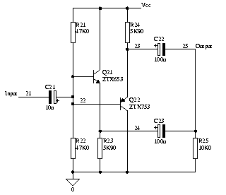
When designed with general-purpose small-signal transistors, the bandwidth ranges from 50 MHz to 250 MHz, necessitating careful grounding and power supply decoupling. The simulation schematic illustrates a two-transistor buffer. Due to copyright issues, models from other sources are not...
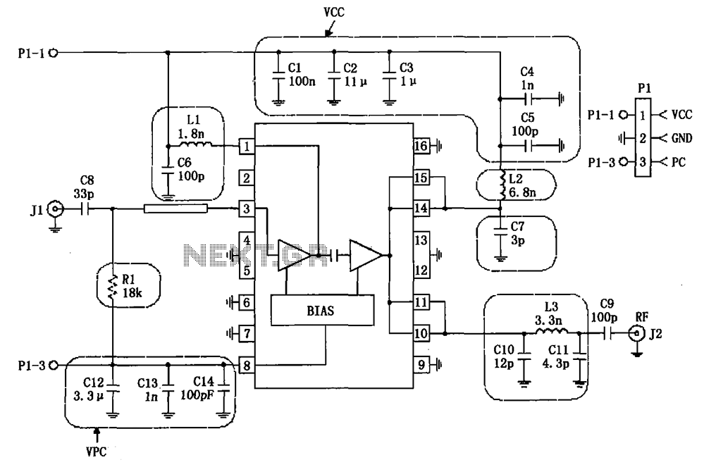
The RF2132 linear power amplifier circuit is depicted in the provided figure. A radio frequency (RF) signal enters through input pin 3 and is processed via a preamplifier. The final stage of the amplifier outputs a gain of 10....
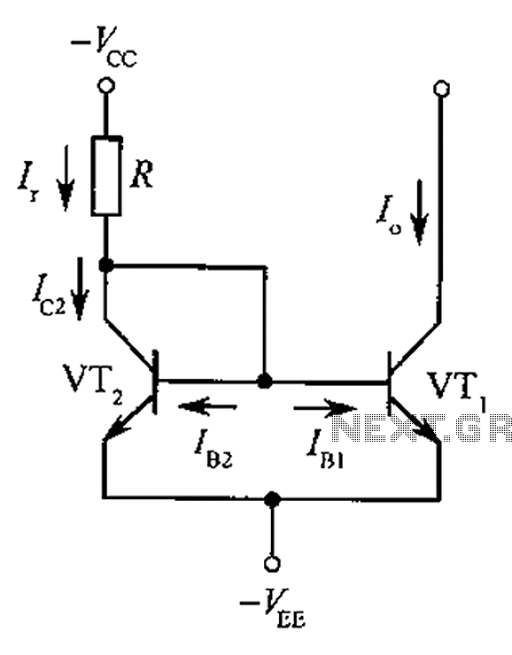
The circuit depicted is a mirror substantially constant current source circuit, in which transistors VT1 and VT2 are matched to each other. The figure illustrates that the current through Ir is equal to Ic2 plus the sum of base...
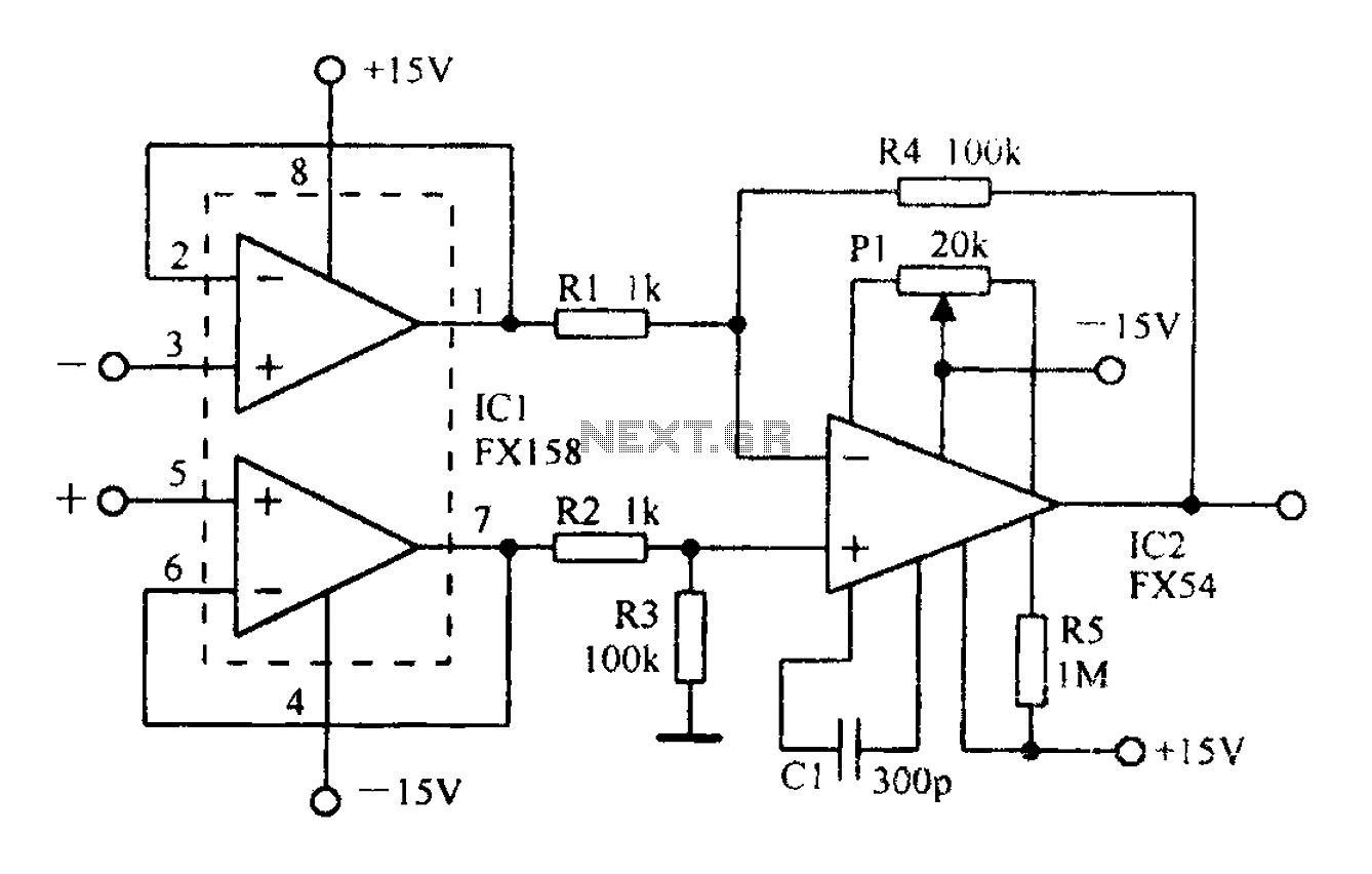
A differential amplifier with input impedance as indicated in the circuit diagram. A differential amplifier is a crucial component in various electronic applications, primarily used to amplify the difference between two input voltages while rejecting any common-mode signals. This characteristic...
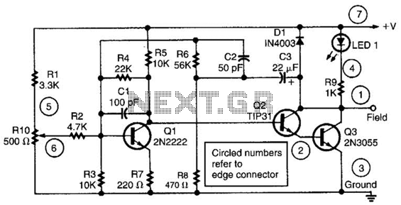
This alternator regulator utilizes a 3-transistor DC amplifier and is designed for a pulled-up field system, where one side of the alternator field returns to the +12V supply, and the other end is pulled toward ground. The circuit monitors...
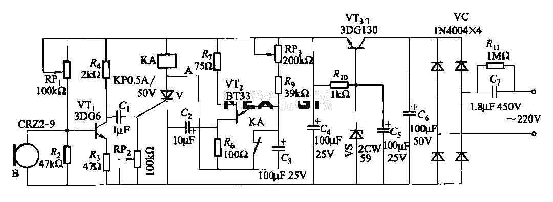
The circuit features voice switches with Figure 2109. It utilizes a single-junction transistor (VT2) and RC components to create a delay. The delay time can be adjusted using the potentiometer (RP3) or the capacitor (C3). The described circuit employs a...