
Transistor Tutorial history sample circuits

The bipolar junction transistor (BJT) is a critical component in modern electronics, functioning as an amplifier or switch in various applications. The device operates through the interaction of two types of charge carriers: electrons and holes, which allows it to amplify signals. In an NPN transistor, electrons flow from the emitter to the collector, while in a PNP transistor, holes move from the emitter to the collector. This fundamental operation is crucial for designing circuits involving signal processing, power regulation, and digital logic.
The manufacturing process of BJTs typically involves a double-diffusion technique, which enhances the efficiency and performance of the device. The NPN and PNP structures are created by alternating layers of N-type and P-type silicon, which are then doped to achieve the desired electrical characteristics. The configuration of these layers directly impacts the transistor's performance metrics, such as gain, bandwidth, and switching speed.
In practical applications, BJTs are characterized by parameters such as current gain (β), collector-emitter saturation voltage (V_CE(sat)), and maximum collector current (I_C). These specifications guide engineers in selecting the appropriate transistor for specific circuit requirements. For instance, the 2N3904 and 2N3906 transistors are commonly used in low-power applications due to their favorable characteristics, including low noise and high gain.
The understanding of BJTs extends into various electronic design fields, where their role in feedback loops, oscillators, and signal modulation is critical. The gain-bandwidth product, a vital parameter in analog circuit design, illustrates the trade-off between gain and frequency response. As the gain of a circuit increases, the bandwidth decreases, necessitating careful consideration in high-frequency applications.
In summary, the bipolar junction transistor remains a foundational element in electronic design, with its principles and characteristics essential for developing reliable and efficient circuits across a range of applications. The continuous evolution of transistor technology, including advancements in fabrication techniques and material science, ensures that BJTs will remain relevant in the ever-changing landscape of electronics.The bipolar junction transistor is still one of the cornerstone`s of modern solid-state electronics. Learn (or review) the basics of this important active device. The Bipolar Junction Transistor (BJT) triggered the revolution in modern solid-state electronics in the 1960`s. Although the discrete small-signal BJT has since yielded to the integrated circuit (IC) in economic importance, it lives on in the form of discrete linear and switching power transistors as well as radio-frequency transistors into the microwave region. The principles behind the operation of the BJT are important to the understanding of many of today`s most popular linear and digital integrated circuits.
Moreover, the transistor families-TTL, Schottky TTL, and emitter-couple logic (ECL) are BJT`s. A BJT is a three-terminal (base, emitter, and collector) device. There are two types: NPN and PNP. Today both are typically made by the double-diffusion process that involves the deposition of two additional layers of doped silicon on a doped silicon wafer. Figure 1-a shows the cross section of an NPN BJT. Its base and emitter terminals are metal depositions on top of the silicon wafer, and its collector is the metalized lower surface of the wafer.
Figure 2-a shows the cross section of a PNP BJT. It is similar to the NPN BJT, except that the N- and P-type materials have changed places. Figure 1-b and 2-b are the schematic symbols for the NPN and PNP transistors, respectively. Notice that they are the same except for the direction of the arrowhead within the symbol at the emitter terminal. This difference will be explained shortly. The term bipolar means that the BJT`s operation depends on the movement of two different carriers: electrons and holes.
In NPN BJT`s the electron is the majority carrier and the hole is the minority carrier. This situation is reversed in the PNP BJT. By contrast, all filed-effect transistors (JFET`s and MOSFET`s) depend upon the movement of only one carrier, either electrons or hoes, depending on whether they are N-channel or P-channel devices, so they are technically unipolar devices. (For more on this, see Electronics Now, April and May 1993). The voltage on the collector of the NPN BJT must be positive with respect to its emitter if current Ic is to flow.
That current will increase with a positive bias on the base. Figure 3-a shows how a small input current applied at the base (Ib) of the NPN BJT can control Ic. The arrowhead indicates the direction of conventional current flow-collector to emitter. Note that it is in the same direction as the arrowhead in the symbol for the NPN transistor. (Electrons flow in the direction opposing the arrowhead. ) Similarly, the PNP transistor requires a negative collector supply with respect to its emitter to operate, and a negative base bias to increase conduction. Fig. 3-b shows conventional current flow in the PNP BJT from the emitter to the collector, as shown in the symbol for the NPN transistor, but opposite to that shown in Figure 3-a.
Most of the common commodity NPN and PNP BJT`s available from electronics distributors and retail stores have been standardized and are made by many different suppliers around the world. Table 1 lists the basic characteristics of two typical general-purpose, small-signal BJT`s that are included in the projects discussed in this article: the 2N3904 NPN-type and the 2N3906 PNP-type.
Both are packaged in small, three-pin plastic cylindrical TO-92 packages with flat faces. The gain-bandwidth product, the frequency at which common emitter forward current gain is unity, applies in the following way: if a transistor in a voltage feedback circuit has a voltage gain of X 100, its bandwidth will be one hundredth of gain bandwidth value. However if the voltage gain is reduced to X 10, the bandwidth will increase to that value divided by 10.
A knowledge of the static and dynamic characteristics of BJT`s will be 🔗 External reference
Related Circuits
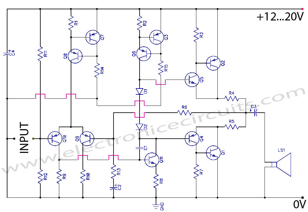
Discrete Class AB Transistor Audio Power Amplifier Circuit Diagram. This is a Class AB transistor power amplifier. It is a simple amplifier. The discrete Class AB transistor audio power amplifier is designed to provide efficient amplification of audio signals while...
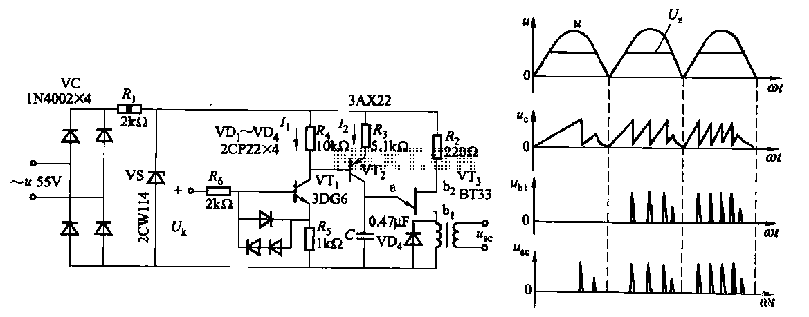
Due to the increased level of the transistor amplifier circuit, the control circuit's performance in Figure 16-6 is more sensitive and can accept input control signals superimposed on others (such as voltage, current, and speed feedback signals) to meet...
This page is provided to the domain owner free by Sedo's Domain Parking. Disclaimer: The domain owner and Sedo maintain no relationship with third-party advertisers. References to any specific service or trademark are not controlled by Sedo or the...
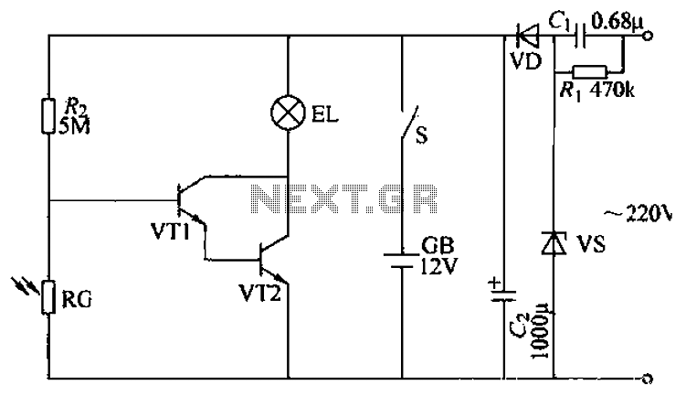
The power supply circuit features a step-down capacitor (C1), bleeder resistors (R), a Zener diode (VS), a full diode (VD), and a filter capacitor (G), along with switches and batteries (GB, SC). The light control circuit is composed of...
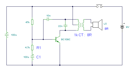
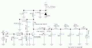
This circuit is a modified Hartley oscillator that incorporates additional components. It utilizes a small audio transformer, specifically the LT700 model. The primary winding is center-tapped with an impedance of 1 kΩ at 1 kHz, while the secondary winding...
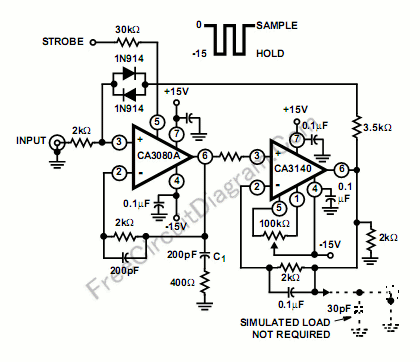
The schematic diagram below illustrates a basic sample-and-hold circuit utilizing the CA3140 as the readout amplifier for the memory capacitor. The CA3080A is also employed in the design. The sample-and-hold circuit is a crucial component in analog-to-digital conversion systems, allowing...