
Transistor Voltage buffer Follower

More: The resistor in the emitter is used to create a voltage from the current passing from the transistor; without it we can't get any voltage as our output would be effectively shorted to ground (0 volts). This circuit's operation is far more predictable and stable than the transistor version, and also requires less external components. Works as described above, no external elements to explain. This circuit uses feedback to maintain the voltage output the same as the input. Note that this schematic does not display power, ground and other connections for the op amp, these vary widely among manufacturers and op amps so refer to your op amp's datasheet for pinouts and power connections. The capacitors that are displayed in the schematic are optional, but very useful to prevent a wrong operation of the circuit, especially in audio or high frequency uses. They stop any DC voltage from moving or otherwise disrupting the bias point of the transistor, thus causing undesired operation. If you build this circuit only with DC, remove the capacitors, as they will prevent the circuit from functioning under those conditions.
The voltage follower, also known as a buffer amplifier, is a critical component in electronic circuits that provides high input impedance and low output impedance. This configuration is particularly useful in applications where the signal source cannot drive the load directly due to impedance mismatch. In the described circuit, a single transistor is employed as the active element, typically a bipolar junction transistor (BJT) or a field-effect transistor (FET), which acts as a buffer between two circuit stages.
The circuit's biasing is achieved using two resistors configured as a voltage divider connected to the base of the transistor. This arrangement sets the operating point of the transistor, ensuring it remains in the active region during operation. The emitter resistor plays a crucial role in establishing the output voltage, as it allows the output to be taken from the emitter, thereby providing a voltage that is a function of the input signal.
The feedback mechanism inherent in the voltage follower configuration allows the output voltage to closely track the input voltage, thus maintaining signal integrity. This is particularly beneficial in audio applications where fidelity is paramount. The optional capacitors mentioned serve to filter out any AC noise that may affect the biasing conditions, providing stability and reducing the risk of distortion.
It is essential to consult the specific datasheet for the operational amplifier or transistor used in the circuit for accurate pin configurations and power supply requirements, as these can vary significantly among different models. Proper implementation of this design can yield a robust voltage follower capable of handling various signal processing tasks while ensuring minimal signal degradation.Two examples of the most common types of Voltage followers (buffers). You can find some theory behind them in our amplifier gain and buffer amplifier pages.his first circuit is a very simple one transistor voltage follower. Consist of two biasing resistors, and one other resistor at the emitter to acquire the output voltage from.
The first to resistors connected to the transistor's base are forming a voltage divider, in order to set a biasing point for the transistor to work in our desired range. Then the transistor, our gain component for the circuit which in this case is only used as a gateway to isolate two circuit stages.
The resistor in the emitter is used to create a voltage from the current passing from the transistor; Without it we can't get any voltage as our output would be effectively shorted to ground (0 volts). This circuit's operation is far more predictable and stable than the transistor version, and also requires less external components.
Works as described above, no external elements to explain. This circuit uses feedback to maintain the voltage output the same as the input. Note that this schematic does not display power, ground and other connections for the op amp, these vary widely among manufacturers and op amps so refer to your op amp's datasheet for pinouts and power connections. The capacitors that are displayed in the schematic are optional, but very useful to prevent a wrong operation of the circuit, specially in audio or high frequency uses.
they stop any DC voltage to move or otherwise disrupt the bias point of the transistor, thus causing undesired operation. If you build this circuit only with dc remove the capacitors, as they will prevent the circuit from functioning under those conditions.
🔗 External reference
Related Circuits
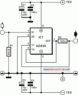
The current source in the diagram reacts very quickly to changes in the input signal and may be utilized in specific measurements. The differential amplifier IC1 ensures that the voltage across resistor R2 is equal to the input voltage,...
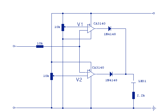
This circuit will provide an indication whenever the input voltage differs from two defined limits, V1 and V2. The supply voltage, Vcc must be higher than the highest input voltage by at least 2 volts. One application here is...
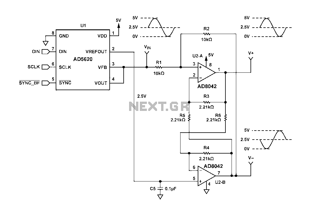
Figure 1 illustrates a circuit that utilizes a single +V power supply and a voltage output Digital-to-Analog Converter (DAC) known as the AD5620. The DAC is controlled via an SPI port, with its output ranging from 0 V to...
The microphone has high sensitivity in the audio range, but in the ultrasonic range, the sensitivity decreases rapidly. The receiver is very sensitive. To prevent overdriving and feedback due to the high sensitivity of the microphone in the audio...
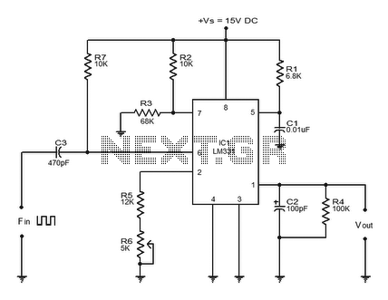
Converter circuits are commonly utilized in various applications, and there are several types available. A simple frequency-to-voltage converter circuit uses the IC LM331, which is essentially a precision voltage-to-frequency converter. This IC has numerous applications, and in this instance,...
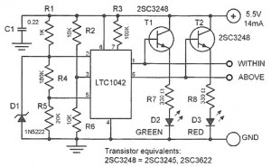
This device is designed to control a supply voltage of +5 V. It provides information signals at TTL levels, accompanied by an LED display that indicates whether the voltage is within the nominal value or deviates from it. The...