
Transistorized Am Radio Circuit

The schematic features a basic AM radio receiver design that leverages the properties of npn transistors for signal amplification and demodulation. The circuit typically consists of an antenna, a tuning circuit, an amplifier stage, and a demodulation section.
The antenna captures radio frequency (RF) signals, which are then filtered and tuned to the desired frequency using an LC circuit composed of an inductor and a variable capacitor. This tuning circuit is crucial as it allows the user to select the specific AM station frequency.
Once the RF signal is tuned, it is fed into the base of the first npn transistor, which acts as a common-emitter amplifier. This stage provides initial amplification of the weak RF signal. The output from this transistor is then connected to the next stage, which may include additional amplification stages or a demodulator.
The demodulation process is typically achieved through envelope detection, where the amplified RF signal is rectified to recover the audio signal. This can be done using a diode connected to the output of the amplifier stage, followed by a low-pass filter to smooth out the rectified signal and extract the audio frequency component.
Power supply considerations are also critical in such circuits, often provided by batteries or a regulated power supply. Bypass capacitors may be included to filter out noise and stabilize the power supply to the transistors.
Overall, this schematic serves as a foundational design for hobbyists and experimenters interested in building their own AM radio receivers, allowing for modifications and enhancements based on specific project requirements. Shown is a schematic of a typical transistor AM radio. This circuit uses npn transistors. The circuit is generic; therefore, no specific values are given for some components. This circuit is for reference, to serve as a starting point for experimenters.
Related Circuits
A good performance is achieved with a two-wire connection for a double touch switch that can function even if there is a break in the left part of the line. This switch is designed for general lighting control, such...
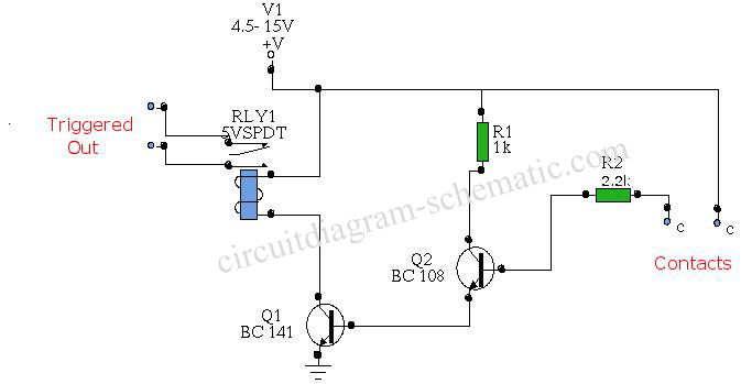
The circuit diagram represents a water-activated relay circuit. This circuit employs two transistors configured as a high-gain compound pair. The transistors used are 2N2222A for T1 and T2, which may also be substituted with BC108. The current gain is...
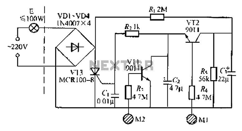
It is said that mice are more sensitive to electromagnetic fields, which is why high-voltage grids generally yield poor results in rodent control. The electronic rodent control system described here does not use high-voltage power lines, thus it does...
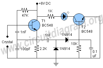
A highly beneficial project involving a crystal tester circuit, also known as an xtal tester circuit, constructed with only a few components. The circuit forms an oscillator that will only oscillate if the crystal under test is functioning properly....
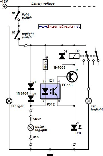
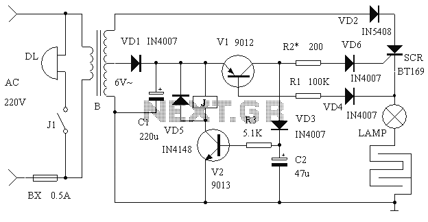
For several years, a rear fog lamp has been mandatory for trailers and caravans to enhance visibility in foggy conditions. When the fog lamp is activated, the fog lamp of the towing vehicle must be turned off to prevent...
The circuit incorporates components Q, C, and ZD, which are responsible for the bias and buffer stages. Its primary objective is to ensure stable MOSFET gate operation and provide an offset voltage through a voltage buffer amplifier stage with...