
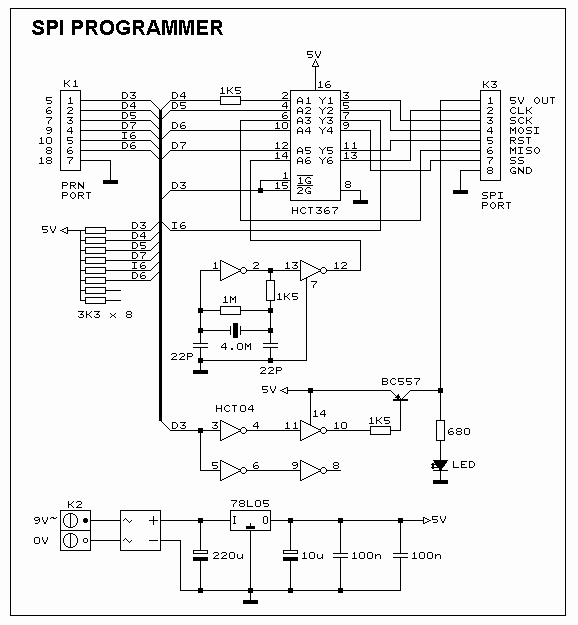
trying to improve on the spi bus

The proposed circuit design effectively addresses the limitations of the SPI bus when connecting multiple slave devices. By implementing a 74HC595 shift register, the circuit can utilize its outputs for slave selection while maintaining the shared SCLK, MOSI, and MISO lines. The shift register's three-state enable pin allows for controlled output activation, enabling seamless communication with individual slaves.
In this configuration, the first transfer over SPI is dedicated to selecting the desired slave device. This is achieved by setting the B0 pin low, which activates the corresponding output on the shift register that is connected to the selected slave's SS pin. Following this, the actual data transfer occurs with B1 set low, ensuring that the data is sent exclusively to the chosen slave. This method simplifies the wiring and reduces the number of required pins on the master device, making it an efficient solution for systems with multiple slave devices.
The schematic for this design should clearly illustrate the connections between the master device, the shift register, and the individual slave devices. Each slave board would have its unique jumper configuration for the shift register outputs, allowing for easy customization and scalability. This design not only optimizes the use of available pins but also enhances the overall functionality of the SPI bus in multi-device applications.Overcome a major drawback of the SPI bus. But to explain this, allow me to go on a little detour first. The I2C bus is an extremely convenient design, because it only needs 4 wires to connect several chips together: Each chip sees the same information, but it works because each chip has been set up to respond only to a specific addre ss on the bus. And that address happens to be conveniently located at the start of each I2C message. With one chip, there`s no problem: one slave select (SS), a serial clock (SCLK), a master-out slave-in (MOSI) pin for outgoing data, and a master-in slave-out (MISO) for incoming data (brilliant naming no confusion!). The trouble is with multiple chips, i. e. slaves. The SCLK, MOSI, and MISO pins can be shared, but not the slave select . Each slave will need a separate pin to select it. And that makes it impossible to use it as a real bus And that`s where yesterday`s post comes in. Suppose we had all the SPI signals, as well as power, as well as two chip selects. Like, eh the SPI/ISP connector, using B0 and B1 as the two select signals how convenient! So here`s the idea: first we send a byte over SPI with B0 set low and then we send the actual data with B1 set low.
The B0 transfer is used to select one specific slave, and the B1 transfer then takes place only with that slave. The good news is that a 74HC595 shift register has all the functionality needed to perform this task, by using the three-state enable pin as a gate to turn the shift register outputs on or off.
Here`s the schematic for it all: The idea is to put this simple circuit on each slave board. On each one, a different output from the shift register gets jumpered. In the above schematic, for example, QD (the 4th bit) has been wired up as slave select. 🔗 External reference
Related Circuits
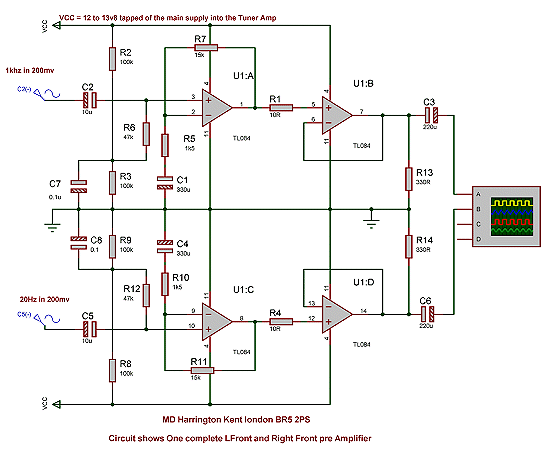
How the circuit works. The circuit comprises a non-inverting amplifier with a final output buffer stage or voltage follower for impedance matching. The described circuit functions as a non-inverting amplifier, which is designed to amplify an input voltage while maintaining...
This SPI Flash Programmer can be utilized for both in-system programming and as a standalone serial flash programmer for Atmel SPI programmable devices. The hardware interface of the programmer is managed through the PC's parallel port, with control signals...
The AMU2481 Audio Mixer is a digital real-time signal processor utilizing NMOS technology, available in a 24-pin DIL plastic package or a 44-pin PLCC package. It is designed for the digital processing of both TV audio information and digital...

When discussing fan control, there are generally two methods: linear control and pulse-width modulation (PWM) control. Linear control is the most commonly used method, which involves reducing the voltage supplied to the fan. For a fan rated at 12...
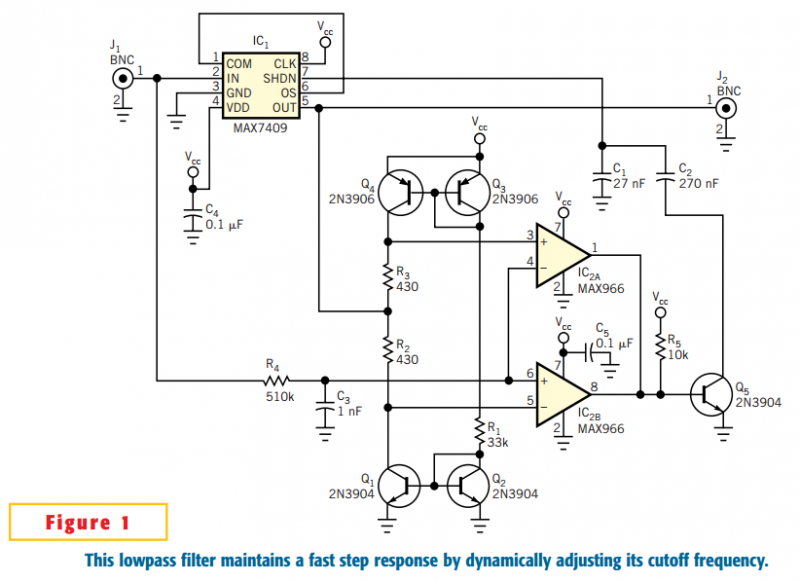
The circuit in Figure 1 accommodates lower cutoff frequencies without sacrificing the step-response time. A window comparator monitors the delta (difference) between the filter's input and output. When the delta exceeds ±50 mV, the filter increases its slew rate...
The spider prop has a straightforward mechanical setup, but its electronic configuration is more complex. It utilizes a stepper motor, which requires a controller, such as a computer or microcontroller, to operate effectively. Stepper motors do not simply turn...