
TV by the photosensitive resistor circuit diagram automatic brightness adjustment

The automatic brightness adjustment circuit for televisions is designed to enhance viewing comfort by adapting the display settings according to ambient light conditions. It employs a photosensitive resistor, commonly referred to as a light-dependent resistor (LDR), which exhibits a change in resistance based on the intensity of light it is exposed to. This component is critical for detecting surrounding light levels.
The circuit architecture integrates the photosensitive resistor with a contrast potentiometer, which serves as a variable resistor to fine-tune the contrast settings of the television. The connection of these components to an intermediate stage allows for the modulation of the voltage signal based on the light intensity detected by the LDR. As the light intensity increases, the resistance of the LDR decreases, leading to a corresponding increase in voltage at the intermediate stage.
The TA7698AP decoding circuit plays a pivotal role in translating the voltage variations into actionable signals that adjust the television's brightness, contrast, and saturation levels. This IC is designed to process the input from the intermediate stage and output the necessary control signals to the television's display driver circuitry.
In scenarios where ambient light is low, the LDR's resistance decreases significantly, causing an increase in the voltage at the potentiometer's midpoint. This change prompts the TA7698AP to modify the display parameters accordingly, ensuring that the image remains clear and visible without excessive brightness or contrast that could lead to viewer discomfort or eye strain.
Overall, this automatic brightness adjustment circuit exemplifies a practical application of analog electronics in consumer devices, promoting enhanced user experience by automatically adapting display settings to environmental changes. By the photosensitive resistor television automatic brightness adjustment circuit shown in Figure photoresistor and contrast potentiometer connected to the intermediate head. U se photoresistor vary light intensity and the change in resistance characteristics, the potential of the intermediate potential head with different light intensity changes, through decoding circuit TA7698AP control, so the TV brightness, contrast, saturation change accordingly. Light brightness, small GR resistance, potentiometer middle of the first potential rise.
Related Circuits
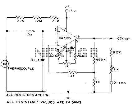
The circuit requires a 15-volt power supply and employs a precision operational amplifier, CA3193 BiMOS, to amplify the generated signal by more than 500 times. Three 22-megohm resistors are utilized to ensure a large-scale output in the event of...
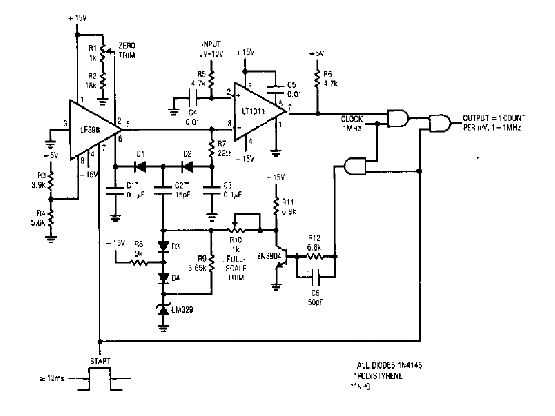
The simple 4-digit converter circuit has an output count of 1, designed to operate within a frequency range of f-IMHz to 10.000. All diodes used in the circuit are IN4146, and the capacitors are made of `POLYSTYRENE` NPO. The...
Low-noise preamplifier circuit. This circuit demonstrates a typical low-noise preamplifier design, which can be utilized to amplify signals from sources such as magnetic heads and microphones within audio applications. The input signal is coupled through a capacitor and subsequently...
At this voltage regulator prototype the maximum current, with output shortcircuited it was only 0.5 A, so no overheating occurred. In this DC voltage regulator circuit, T1 is for current limitation. As soon as the voltage on the R2...
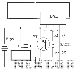
The circuit operation principle of the device illustrated in Figure 13 is as follows: When the barbed wire (Fe) remains intact, the output pin (O) of the LSE is at a high state. Consequently, the transistor (VT) remains off,...
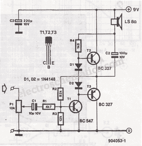
This miniature audio amplifier provides an output of up to 250mW and can function as a final stage audio amplifier for radio sets. The schematic is straightforward, featuring one BC transistor. The described miniature audio amplifier is designed for efficient...