
Ultrasonic switch

The circuit operates in two primary sections: the transmitter and the receiver. The transmitter utilizes the NE 555 timer IC configured in astable mode, generating a continuous square wave at 40 kHz. This frequency is suitable for ultrasonic applications, ensuring that the transmitted signal is above the audible range for humans. The output from the NE 555 is fed into a pair of transistors (Q1 and Q2), which serve as a push-pull amplifier configuration, effectively boosting the signal strength before it is emitted by the ultrasonic transmitter (K1). The push-button switch (S1) allows for manual activation, ensuring that the transmitter operates only when desired.
In the receiver section, the ultrasonic transducer (K2) is responsible for detecting the ultrasonic waves reflected from nearby objects. Upon receiving an ultrasonic signal, K2 generates a small voltage proportional to the intensity of the signal. This signal is often too weak for further processing, which is why it is amplified using a two-stage transistor amplifier (Q3 and Q4). The amplified output is then rectified using diodes D3 and D4, converting the AC signal into a DC voltage suitable for further analysis.
The rectified voltage is sent to the inverting input of an op-amp configured as a comparator. This setup allows for threshold detection; when the voltage exceeds a certain level, indicating the presence of an ultrasonic signal, the comparator output switches state. This change in output activates transistors Q5 and Q6, which control a relay. The relay can switch larger loads, enabling practical applications such as activating alarms or other devices based on the presence of an object detected by the ultrasonic signal.
Diode D5 plays a critical role in protecting the circuit by allowing current to flow back to the power source when the relay coil is de-energized, preventing potential damage to the transistors from back EMF generated by the relay coil. Overall, this circuit design demonstrates an effective method for utilizing ultrasonic technology in various applications, including proximity sensing and object detection.The transmitter part of the circuit is build around IC1(NE 555). The IC1 is wired as an astable multi vibrator operating at 40KHz. The output of IC1 is amplifier the complementary pair of transistors ( Q1 & Q2) and transmitted by the ultrasonic transmitter K1. The push button switch S1 is used the activate the transmitter. The receiver uses an ultras onic sensor transducer (K2) to sense the ultrasonic signals. When an ultrasonic signal is falling on the sensor, it produces a proportional voltage signal at its output. This weak signal is amplified by the two stage amplifier circuit comprising of transistors Q3 and Q4.
The output of the amplifier is rectified by the diodes D3 & D4. The rectified signal is given to the inverting input of the opamp which is wired as a comparator. When ever there is an ultrasonic signal falling on the receiver, the output of the comparator activates the transistors Q5 & Q6 to drive the relay. In this way the load connected via the relay can be switched. The diode D5 is used as a free wheeling diode. 🔗 External reference
Related Circuits

This circuit illustrates the LM2576T integrated circuit (IC) step-down switching power supply circuit diagram. Features include a 60V input voltage with output options of 3.3V, 5V, 12V, and 15V. The LM2576T is a popular voltage regulator known for its ability...

This project presents numerous practical applications in security and alarm systems for homes, shops, and vehicles. The circuit is highly sensitive and can be configured to either reset automatically or remain triggered until manually reset after an alarm. It...

The proximity switch circuit consists of the HMC1001 sensor, operational amplifier (AMP04), and a light-emitting diode (LED). The operational amplifier functions as a comparator. When a magnet, measuring between 6mm and 12mm, is moved to a predetermined position near...
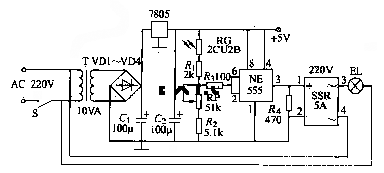
The NE555 time base circuit with an AC solid-state relay (SSR) can function as an automatic light switch circuit. The circuit diagram illustrates that during the day, the incandescent light is turned off due to the influence of the...
After turning off TT2, the input signal enters through chi Az, where the input resistance is very high and reaches the same potential. The inverting input terminal must also be associated with this movement. Therefore, Trr functions as a...

Techniques for an echo sounder used to measure ocean depth can be implemented with an ultrasonic distance measuring device. This device uses a circuit similar to the one described in the previous article, which includes a series of ultrasonic...