
Universal adder 741 1458 schematic

The inverting adder circuit is a fundamental operational amplifier (op-amp) configuration used to perform the addition of multiple input signals. In this configuration, the op-amp is connected in an inverting mode, where the inputs are applied through resistors to the inverting terminal. The non-inverting terminal is typically grounded.
In the inverting adder circuit (Figure a), the output voltage (Vo) is a negative sum of the input voltages (Vi1 and Vi2), scaled by the feedback and input resistors. The relationship can be mathematically expressed as Vo = - (Vi1 + Vi2), indicating that the output is inverted relative to the sum of the inputs. The resistors connected to the input terminals determine the gain of each input signal. If the resistors are equal, the outputs will be inversely proportional to the inputs.
For phase addition, the circuit depicted in Figure (b) employs a different configuration that allows for the summation of input signals without inversion. In this case, the output voltage is given by Vo = (Vi1 + Vi2), which directly represents the algebraic sum of the input voltages. This configuration typically involves a non-inverting summation approach, where the op-amp is configured to add the inputs in phase, resulting in a positive output that reflects the total of the input signals.
Both configurations are widely used in analog signal processing applications, such as audio mixing, data acquisition systems, and various forms of signal manipulation where the summation of multiple signals is required. Proper selection of resistor values and op-amp specifications is crucial to ensure desired performance, including bandwidth, slew rate, and output drive capability. As shown for the common addition circuit. Figure (a) is the inverting adder circuit, an input-output relationship is: Vo - (Vil + Vi2) When you need to phase addition, the circ uit shown in Figure may be used (b), the input-output relationship is: Vo Vil + Vi2
Related Circuits
All integrated circuits (ICs) are equipped with a 0.1 µF monolithic ceramic capacitor connected across their terminals. Additionally, each board features two capacitors: a 10 µF tantalum capacitor and a 100 µF electrolytic capacitor. The START BUTTON serves as...
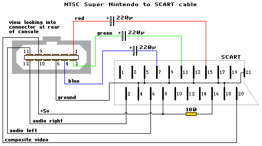
The schematic diagram is similar to the SNES NTSC RGB cable, with the only modification being the addition of capacitors to the RGB line. The diagram is accurate, but it does not include capacitors. A GameCube SCART lead can...
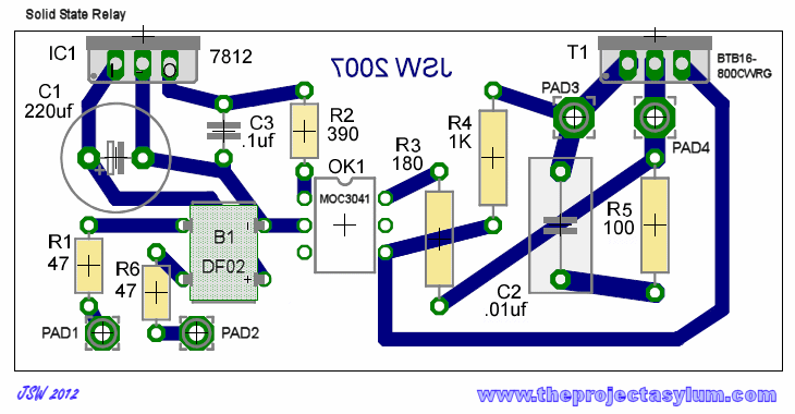
This solid-state relay circuit operates using 120 volts from household mains and should only be constructed by individuals with the necessary knowledge and skills to ensure safety. Failure to do so may result in personal injury or property damage. The...
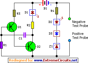
This simple circuit tests speakers, microphones, transformers, and voltage. It is essentially a very low-frequency oscillator that produces extremely short pulses. The sound produced is easy to hear and helps determine the precise direction it originates from, making it...

Two identical integrated circuits, U1 and U2, known as "hex inverters," are utilized for the primary functions of the theremin. These are CMOS (Complementary Symmetry Metal Oxide Semiconductor) devices commonly employed in digital circuits to perform a logic function...

Connect the components, ensuring to pay attention to the connections for the transistor. The 22-ohm load resistor and thermistor should be connected in a manner that allows for good thermal contact. Note: If using the Light Application Adapter, REFIN-...