
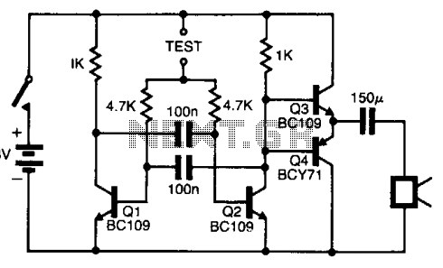
Universal Test Probe

The compact test probe circuit is designed for efficient voltage measurement across various electronic components, providing a user-friendly interface through the use of LED indicators. The circuit operates by comparing the voltage at two pins, A (reference) and B (measured), allowing for quick assessment of component functionality. The illumination of LEDs serves as a visual cue for different voltage ranges, enabling technicians to quickly diagnose issues without needing to interpret numerical values.
The use of transistor T5 as a zener diode is a notable feature, allowing for voltage clamping and protection against over-voltage conditions. This configuration ensures that the circuit remains safe even when subjected to high input voltages, particularly when R1 is rated for higher power dissipation. The choice of a 0.5-W resistor allows for a maximum input voltage of 200 Vrms, making the probe suitable for a wide range of applications, including testing in industrial environments.
Additionally, the circuit's design minimizes power consumption, drawing a maximum of 10 mA during operation, which is efficient for battery-powered applications. The quiescent current draw of approximately 5 mA further enhances the usability of the probe, eliminating the need for a manual on/off switch and allowing for continuous readiness without significant battery drain.
Overall, this compact test probe circuit exemplifies a practical solution for quick voltage measurements in various electronic applications, combining functionality, safety, and efficiency in a single device. The compact test probe provides rapid "measurement" of voltage levels at digital gates, fuses, diodes, batteries, and others. It does not provide absolute values, but rather it provides a good indication of correct operation or otherwise. Measurements are carried out with pins A and B. If the potential difference between A (the reference pin) and is 1.9 to 2.0 V, D2 will light. If the voltage at is < 1.4 V higher than that at A, D3 will light. Finally, if the potential at is > 11 V, with respect to that at A, Dl will light. Transistor T5 is used as a zener diode. The probe allows the measurement of alternating voltage. The maximum input voltage is highly dependent on the dissipation allowed in Rl. For example, when this resistor is a 0.5-W type, the input voltage can be as high as 200 Vrms. The current drawn by the circuit depends on the number of lighting LEDs: it is not more than 10 mA at a supply voltage of 3 V.
In quiescent operation, the current is so low (about 5 ) that an on/off switch is not necessary.
Related Circuits
The machine model, commonly used for ESD testing in Japan, is a more severe ESD test. This model simulates metallic contact between the device under test and a charged body. The source capacitor is 200pF with no limiting resistor....
The pitch of the tone is dependent upon the resistance under test. The tester will respond to resistance of hundreds of kilohms, yet it is possible to distinguish differences of just a few tens of ohms in low-resistance circuits....

This is a minimum component complete Universal Counter. It can use input frequencies up to 10 MHz at INPUT A and 2 MHz at INPUT B. If the signal at INPUT A has a very low duty cycle, it...
This logic probe utilizes a single CMOS integrated circuit (IC) to indicate three logic states: High, Low, and Pulsing. If the probe input is in a high impedance state, which occurs when it is not connected to a circuit,...

When the time delay expires, SCR1 conducts and removes the gate signal from SCR2, which stops the motor. Both the time delay and motor speed are adjustable by potentiometers R2 and R3. If heavier motor loads are anticipated, use...
This 40 kHz crystal-controlled oscillator circuit drives an infrared LED with powerful 40 mA pulses. The circuit operates at a frequency of 40 kHz, determined by the crystal oscillator, which provides stable frequency output essential for applications requiring precise timing....