
Use of one hour LM122 timer circuit

The LM122 timer circuit is designed to perform a variety of timing functions based on the configuration of its components. The circuit typically includes a capacitor (C), a resistor (R), and two switches (S1 and S2). The LM122, a versatile timer IC, operates by charging and discharging the capacitor through the resistor, which determines the timing intervals.
Upon activation by switch S1, the timer begins its cycle. The capacitor charges through the resistor, and the voltage across the capacitor increases until it reaches a predetermined threshold, at which point the timer output toggles. This output can be used to control other devices or components in the circuit.
Switch S2 serves as a control mechanism that can halt the timing process at any point. When S2 is in the off position, the circuit is effectively disabled, preventing any further timing operations. However, once S1 is activated again, the timer resumes its operation from the point it was stopped, allowing for flexible timing control.
The behavior of the circuit during the discharging phase is critical. When the capacitor discharges, the voltage at the R/C terminal drops to zero, indicating that the timer is ready to receive a new start signal. The design ensures that the timer's operational state does not change during the reset process, which is crucial for maintaining the integrity of the timing function.
In summary, the LM122 timer circuit is a robust design that allows for precise timing control through the strategic use of switches and passive components. Its ability to handle interruptions and resume timing operations makes it suitable for a variety of applications where timing accuracy is essential. As shown in Figure 1 hour using a LM122 timer circuit. Start of the circuit, reset and stop halfway, etc. are converted by the switching operation. Figure, S1 to start timing w hen the timer is started, then this switch has no effect. S2 is centrally located in the off switch, the timer can switch through the conversion is completed: Charge - open - discharge. Since midway stop charging, even if not to the timer set time, the charging station will return to work status timer output lines.
When the C discharge, R/C terminal voltage is zero, the discharge position waiting for start signal S1. Even if the recovery position. Work status timer output line does not change, therefore, the timer is reset when the work which the state remains the same output line, in this moment, C starts charging again, start a timer to change working hours.
Related Circuits
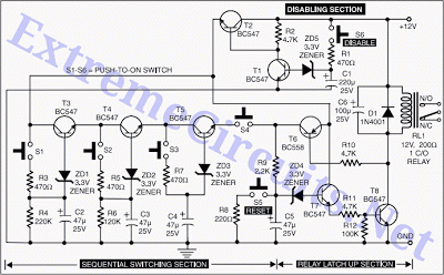
This intelligent electronic lock circuit is constructed using only transistors. To unlock this electronic lock, the user must press tactile switches S1 through S4 in sequence. For added security, these switches can be labeled with different numbers on the...
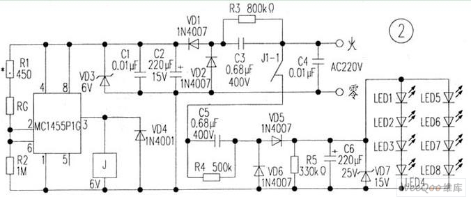
The circuit is depicted in Figure 1, while the electrical schematic diagram is presented in Figure 2. The AC voltage of 220V is reduced by components C3 and R3. The diodes VD1 and VD2 rectify the voltage, and capacitors...
The Audio Automatic Gain Control (AGC) circuit monitors the output signal level of an audio preamplifier. When the input signal increases, the AGC circuit automatically reduces the amplifier's gain. Conversely, when the input signal decreases, the AGC circuit increases...

Here is a small LM386-based square-wave oscillator constructed from the following schematic. A 50k potentiometer was used in place of a 30k resistor, which functions as a pitch controller. The audio provided consists of track recordings made in Ableton...
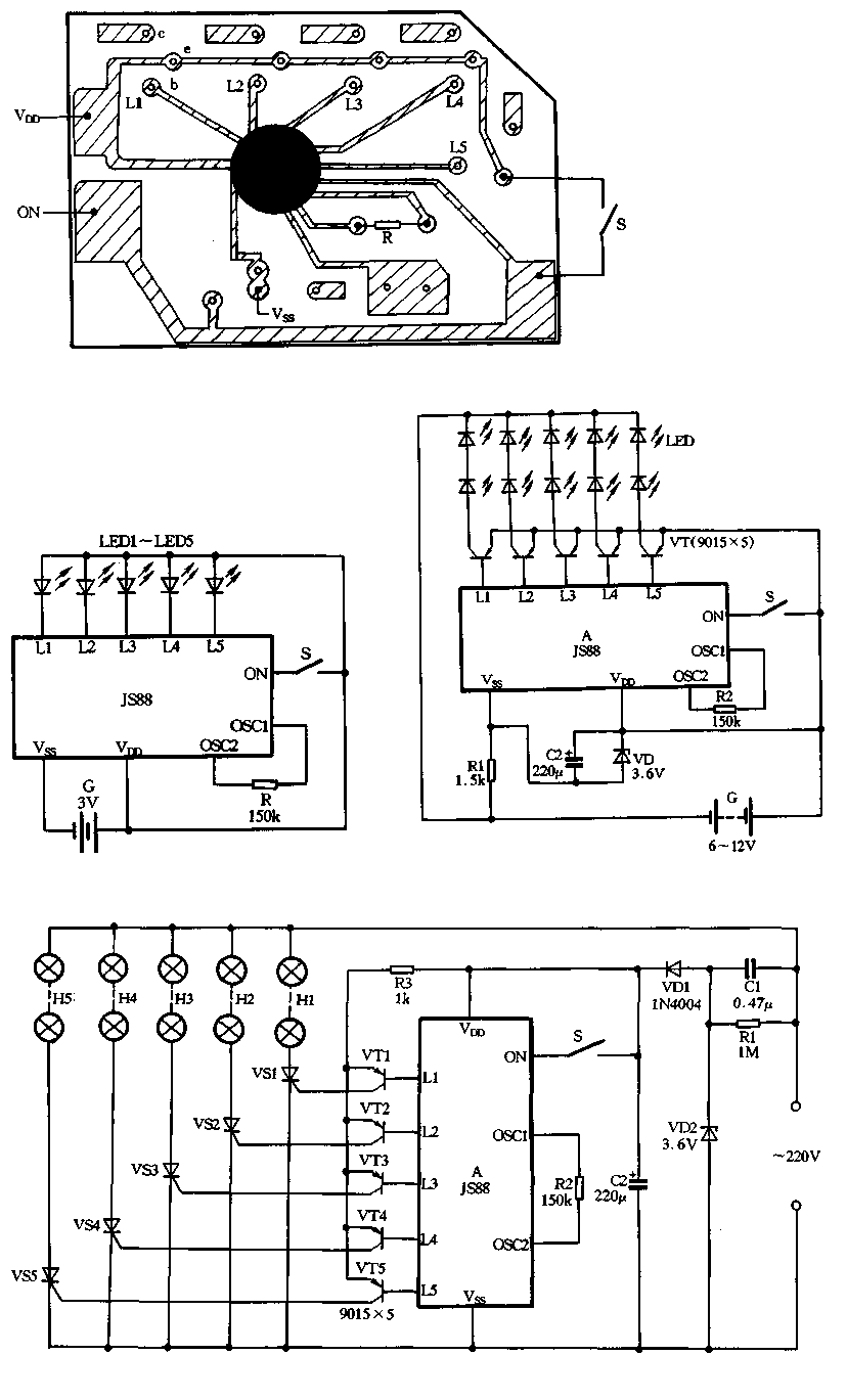
Figure 2-39 illustrates a typical application circuit for the JS88 manifold, which includes an oscillation resistor (R) that allows for fine-tuning of the water flicker frequency. When switch (S) is closed, components L1 to L5 sequentially output low signals...
Amplification is utilized to convert video output signals from various devices, such as VCRs and DVD players, which often require amplification of weak output signals. Additionally, it can transmit radio frequency signals over a radius of approximately 7 meters,...