
Used in conjunction with multimeters FET Vp Vas checker

The described circuit involves an operational amplifier (op-amp) configured to achieve a specific gain and feedback mechanism, which is crucial for precise control in applications such as biomedical instrumentation. The feedback loop is designed using a Field Effect Transistor (FET), where the input resistance plays a pivotal role in stabilizing the circuit's performance by determining the roll-off characteristics of the current.
The FET drain current is modulated through a determination circuit, which ensures that the output voltage remains stable and accurately reflects the input conditions. This method is particularly useful in simulating biological signals, such as those found in fake blood circuits, where the output must closely mimic physiological responses.
The inclusion of a Zener diode serves a dual purpose: it provides a stable reference voltage of 9V, which is essential for the accurate measurement of pressure in the circuit, and it protects the circuit from voltage spikes that could lead to malfunction or damage. The pressure clamp is integral in ensuring that the circuit operates within safe voltage levels, thereby enhancing reliability.
A limiting resistor is strategically placed to control the gate current, preventing excessive current flow that could lead to component failure. This resistor ensures that the FET operates in its optimal region, allowing for efficient signal processing with minimal power loss. The overall design emphasizes precision, stability, and safety, making it suitable for sensitive applications in electronic instrumentation. Chen is in the OP put too amplifying circuit, so that the comb over current feedback loop with input resistance determined current roll, so FET drain current, a gate by the det ermination circuit Ren V es. That fire is output 0P what constitutes fake blood circuit, with A, the potential of the inverting input terminal of the control to make it equal to zero. A zener diode D. And D, produce 9 VBijIU pressure measured object (DU gate T) of [h pressure clamp, the circuit is not to force abnormal voltage.
R. It is limiting resistor to control the gate cast rb stream, so e, too to people (usually almost no electric current flows through).
Related Circuits
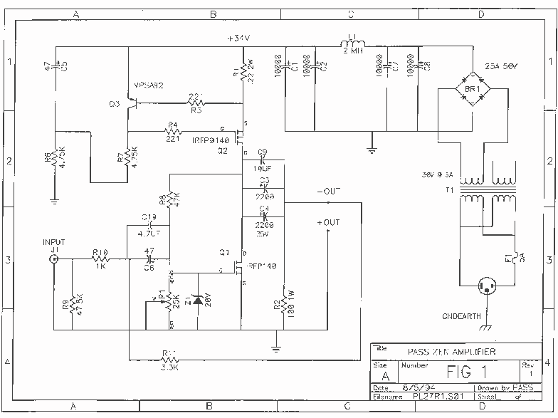
The Zen single-ended MOSFET amplifier was published by Nelson Pass in The Audio Amateur. In a subsequent issue of this magazine, Nelson slightly improved the original design. The "Revisited" version includes the following circuit modifications: 1. More extensive power supply...

This circuit is a FET Cascode Video Amplifier. The cascode amplifier FET used for video applications has a very low input impedance and nearly zero feedback reduction. The 2N3823 transistor was selected due to its low capacitance and high...
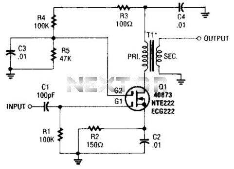
A MOSFET is utilized as a wideband buffer amplifier. T1 is wound on a toroid of approximately specified diameter, using material suitable for the frequency range, typically between 1 MHz and 20 MHz. The turns ratio should be approximately...
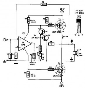
This audio power amplifier employs two complementary MOSFETs (IRF9520 and IRF520) to provide up to 20W output into an 8-ohm speaker. A TL071 operational amplifier functions as the input amplifier. The MOSFETs require heatsinking with a thermal resistance of...

Protect home appliances from voltage spikes using this simple time delay circuit. This circuit activates when power to the appliances is switched on or resumes after a power outage. The time delay circuit is designed to safeguard sensitive electronic devices from...
The circuit described is a single JFET design that provides limited gain. By incorporating a source resistor bypass capacitor, the gain can be significantly enhanced, resembling a single stage of the original tube preamp used in guitar amplifiers. It...