
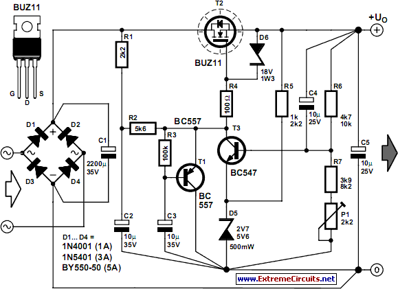
variable 4 a25v power supply

The circuit design is structured in three distinct stages, each serving a specific function essential for the overall operation of the power supply. The first stage initiates the process by utilizing a transformer to step down the input voltage to a safer level. This is followed by a bridge rectifier, which converts the alternating current (AC) output from the transformer into direct current (DC). The 10,000 µF electrolytic capacitor plays a critical role in smoothing the rectified voltage, effectively filtering out ripples and providing a stable DC output suitable for subsequent stages.
In the second stage, the circuit employs BC327 transistors, which are bipolar junction transistors (BJTs) known for their efficiency in switching and amplification applications. These transistors are integrated with additional components to form a reference voltage generator. The reference voltage is crucial as it sets the operating conditions for the driver transistor. The inclusion of a potentiometer allows for adjustable voltage levels, providing flexibility in the output power. The configuration of a top resistor in conjunction with the potentiometer ensures precise control over the voltage applied to the driver transistor, thereby regulating the power output.
The design features a resistive and non-switched control mechanism, which results in a pulsed voltage at the emitter of the driver transistor. This pulsed output is vital for applications requiring variable power levels. To ensure the integrity of the output signal, a small output filter, consisting of an electrolytic capacitor, is incorporated at the output terminals. This filter mitigates any high-frequency noise, ensuring a clean and stable output voltage.
In summary, this circuit design effectively combines isolation, voltage regulation, and filtering to produce a reliable variable power supply capable of delivering up to 4 A at 25 V. The schematic serves as a valuable reference for understanding the intricate workings of the power supply and the roles played by each component within the circuit. Further insights and details can be explored on the dedicated webpage, enhancing comprehension of the circuit's functionality and applications.As shown in the scheme that the circuit consists of three stages. The first (which is formed by a transformer, bridge rectifier and an electrolytic capacitor 10000 F) is responsible for isolating and reduce the voltage, improve and filter. The second phase (consisting of, BC327 transistor integrated circuits and components attached) is responsibl
e for providing a reference voltage which is used to determine, together with the potentiometer and top resistor, voltage applied to the driver transistor and power. It should be noted that they made a resistive and non-switched control (switching) so the voltage at the emitter is pulsed.
Then we have a small output filter formed by the electrolytic capacitor and terminals. The schematic diagram come from circuit: Variable 4 A/25V Power Supply power supply. Go to that page to read the explanation about above power supply related circuit diagram. 🔗 External reference
Related Circuits
The circuit diagram illustrates a voltage regulator designed from discrete components to meet specific voltage requirements. It provides two sets of component values for output voltages of 6.3 V (upper) and 12.6 V (lower). The components used include BC547...
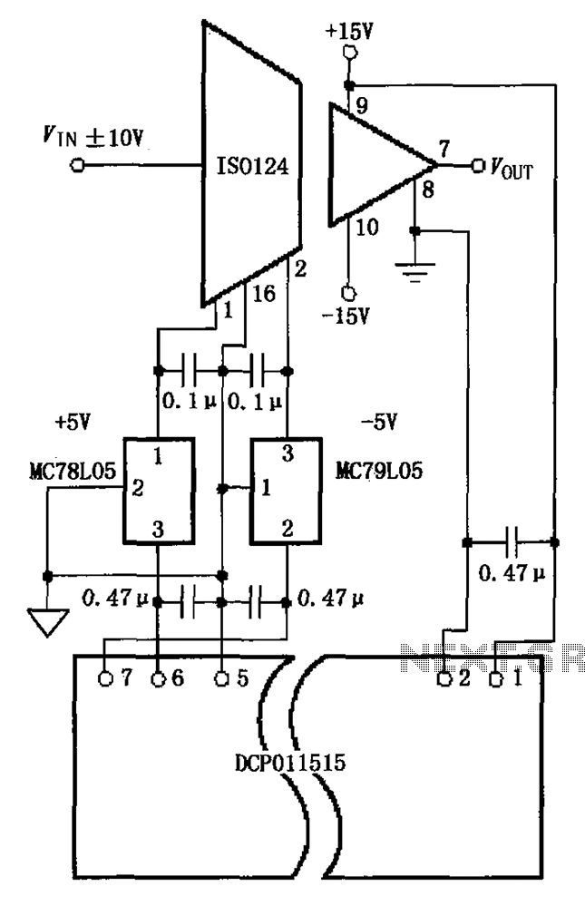
The circuit depicted in the figure includes the ISO124 and MC78L05 components, along with an external regulator, MC79L05, and the DCP011515, which collectively enhance the power supply rejection ratio (PSR) of the circuit. The input signal, VIN (maximum swing...
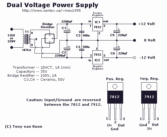
This circuit is a dual voltage regulated power supply, +12, -12, 0 volt. It uses the 7812 and 7912 regulators. You need a 18VCT, 1A transformer at input. More: Caution: Input / Ground are reversed between the 7812 and...
This document provides a step-by-step guide for modifying a disposable camera flash unit to serve as a power supply for a Geiger tube. The process involves removing the flash tube and trigger transformer from the circuit board by gently...

The circuit utilizes a transistor (VT) and a voltage regulator (VSL) to create a constant current source, employing three regulators to enhance the performance of the regulator circuit. The described circuit employs a transistor (VT) in conjunction with a voltage...
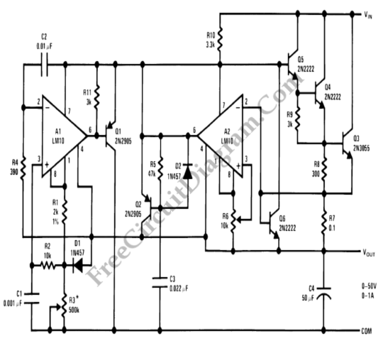
A laboratory power supply is characterized by its wide adjustable voltage range and robustness. Continuous voltage adjustment is necessary, as well as a current limiter for safety and reliability. A suitable design can be created using the LM10 operational...