
Vco

The described circuit utilizes a timer IC configured in astable mode, which produces a continuous square wave output. At the start, the voltage at pin 2, which serves as the trigger input, is lower than the defined threshold, initiating the timer operation. The rapid charging of capacitor C through diode D1 and resistor R1 is crucial for the timing characteristics of the circuit. The choice of resistor R1 and the capacitance of C will determine the charge time, influencing the frequency of the output waveform.
When the voltage across capacitor C reaches 2/3 of the supply voltage (VDD), it triggers the reset of the flip-flop inside the timer IC. This action causes the output on pin 3 to drop, leading to the discharge of capacitor C. The discharge path is facilitated by the current mirror TLO11, which ensures a controlled discharge rate, thereby stabilizing the output.
The cycle repeats when the voltage at pin 2 reaches 1/3 VDD, which serves as the lower threshold for triggering the timer again. This mechanism creates a self-sustaining oscillation, where the timer continuously alternates between charging and discharging the capacitor, resulting in a square wave output. The frequency and duty cycle of the output can be adjusted by varying the values of R1 and C, allowing for flexibility in applications such as pulse generation, timing circuits, or clock signals in digital systems.At startup, the voltage in the trigger input at pin 2 is less than the trigger level voltage, "13 VDD. caus ing the timer to be triggered via pin 2. The output of the timer at pin 3 becomes high, allowing capacitor c, to charge very rapidly through diode Dl and resistor Rl.
When capacitor C, charges to the upper threshold voltage 2 /3 V00, the flip-flop is reset, the output at pin 3 decreases, and capacitor C, discharges through the current mirror, TLOll. When the voltage at pin 2 re-dches 1/3 VDD. the lower threshold or trigger level, the timer triggers again and the cycle is repeated.
Related Circuits
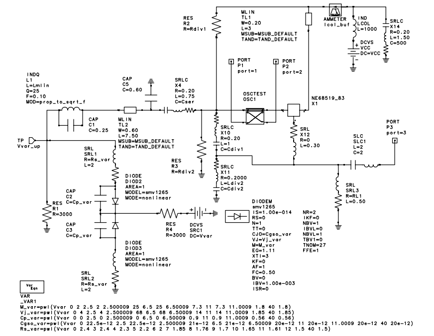
Modern set-top DBS TV tuners require high performance, broadband voltage control oscillator (VCO) designs at a competitive cost. To meet these goals, design engineers are challenged to create high performance, low-cost VCOs. Broadband voltage control oscillators (VCOs) are vital components...
The output frequency of this simple, low-cost active voltage-controlled oscillator circuit is based on the inherent frequency-dependent characteristics of an operational amplifier. The oscillator circuit utilizes a TL082 op-amp. Upon application of power, the circuit generates a sinusoidal wave....
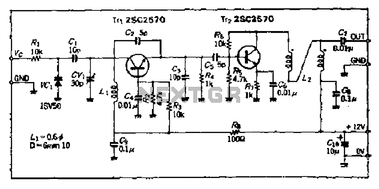
The Bong circuit is a high-frequency Colpitts oscillator that utilizes a Ge coil (L). It features two heads and is designed for simple production. The frequency of oscillation can be determined, and testing is conducted to ascertain the value...
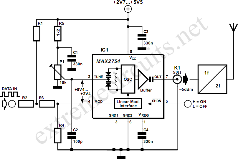
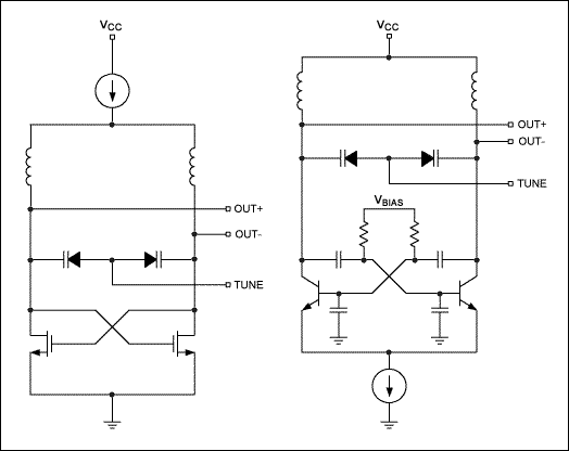
High-frequency voltage-controlled oscillators (VCOs) are challenging to construct, which is why Maxim has developed the integrated 1.2 GHz oscillator, the MAX2754. The center frequency is adjustable via the TUNE input, while a linear modulation input allows for frequency modulation....
The LA4165M Recording-Playback Integrated Circuit (IC) integrates the necessary functions to design recording and playback systems, as well as motor control circuits, for both micro and standard cassette tape recorders into a single chip. It features automatic audio input...
This document tracks the history of voltage-controlled oscillators (VCOs) since around 1910 and provides examples of VCO integration in RF integrated circuits (ICs). Voltage-controlled oscillators (VCOs) are critical components in various electronic systems, particularly in radio frequency (RF) applications. A...