
Video enhancement circuit diagram
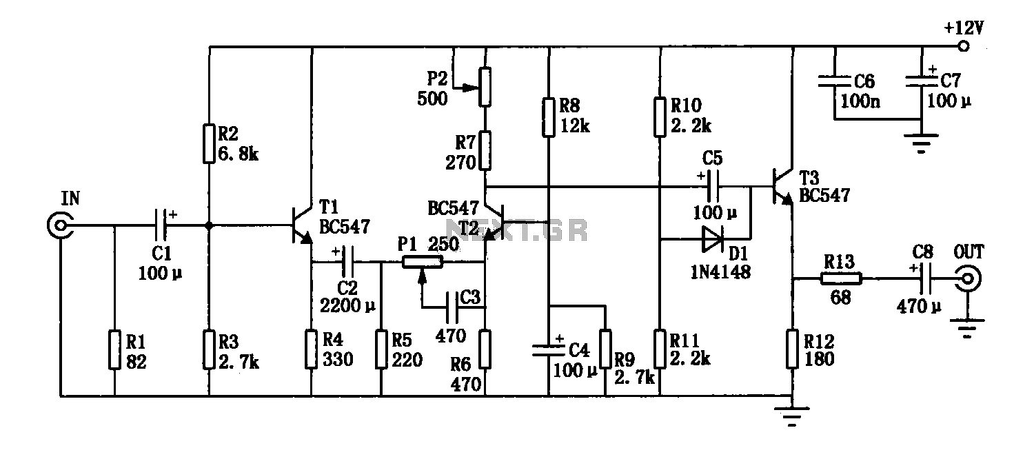
The enhancement circuit is designed to improve the quality of video signals by amplifying high-frequency components, which are crucial for image clarity and contrast. The circuit operates by connecting the output between a VCR and a television's SCART input, facilitating seamless integration into existing setups. The use of transistor T1 serves to dampen unwanted signals, ensuring that only the desired frequencies are amplified.
Resistor R1 is critical in maintaining an input impedance of approximately 75 ohms, which is standard for video signals, allowing for optimal signal transfer and minimizing reflections. The amplifier stage, represented by transistor T2, is where the main signal amplification occurs. The gain of this stage is adjustable through potentiometer P2, which provides flexibility for varying input signal strengths. The frequency response of T2 is shaped by the interaction of components P1, R6, and C6, allowing users to tailor the circuit's performance to their specific needs.
Transistor T3 functions as a buffer, ensuring that the circuit can drive a standard 75-ohm load effectively. This is important for maintaining signal integrity when interfacing with other equipment. The output level can be fine-tuned using potentiometer P2, allowing for an output of 1 Vp-p, with the expectation that the open-circuit output will reach 2 Vp-p. This design not only enhances the visual quality of the television image but also provides users with the ability to customize their viewing experience.Enhancement circuit as shown in the high-frequency component of the video signal can be increased, thereby enhancing the contrast of the TV image, it can also be connected to t he output terminal between the VCR and the TV SCART input. Circuit transistor Tl dampening effect. The resistance Rl ensure enhanced input impedance of the circuit is approximately 75. Signal applied to the amplifier stage T2, the gain depends on the position of the potentiometer P2. T2 signal frequency characteristics of the base by Pl, R6, C6 constraints, and therefore to some extent, controllable by the user (via Pl). T3 buffer stage provides sufficient current for properly driving the vast majority 75 load. Adjust the potentiometer P2, the output is 1Vp-p (open-circuit output level should be 2Vp-p).
Related Circuits
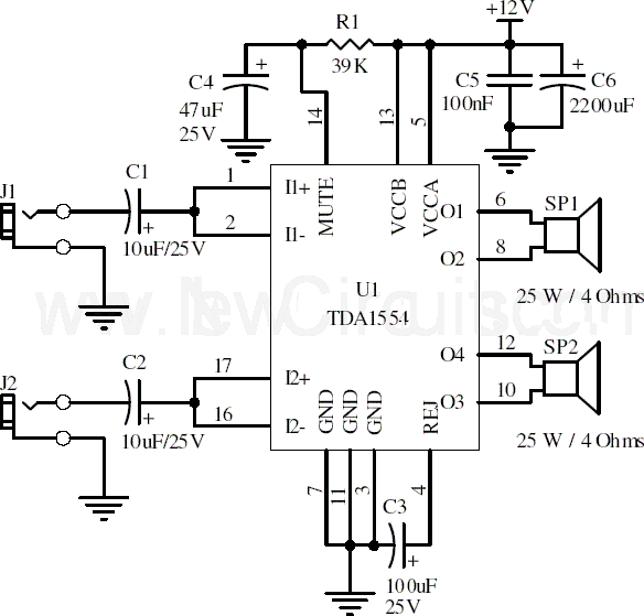
This document presents a 22-watt stereo audio power amplifier circuit diagram utilizing the TDA1554 integrated circuit from NXP Semiconductors (formerly known as PHILIPS Semiconductors). The circuit is designed to amplify stereo signals effectively. It dissipates approximately 28 watts of...
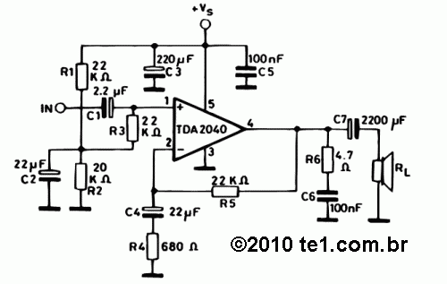
The TDA2040 is a monolithic integrated circuit housed in a Pentawatt package, designed for use as an audio class AB amplifier. It typically delivers an output power of 22W (with a distortion factor of 0.5%) at a supply voltage...
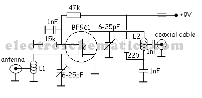
A simple and cost-effective TV antenna amplifier circuit is constructed using the BF961, a dual-gate N-channel MOSFET, which serves as the input and mixer stages. The described TV antenna amplifier circuit utilizes the BF961 dual-gate N-channel MOSFET due to its...
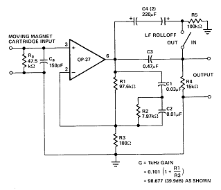
The circuit contributes 3.2 nV/√Hz of voltage noise and 0.45 pA/√Hz of current noise. To minimize noise from other sources, resistor R3 is configured to 100 ohms, resulting in an additional voltage noise of only 1.3 nV/√Hz. Resistors R1,...
This design circuit is for a mass air flow (MAF) sensor. The MAF sensor converts the volume of air entering the engine into a voltage signal. The main components of the MAF sensor include a thermistor, a platinum hot...

The circuit illustrated in Figure 3-136 incorporates a limit switch (SQ) that, when the motor operates a mechanical device to reach a predetermined position, cuts off the power and initiates dynamic braking for fast and accurate positioning. This configuration...