
VLQC circuit

The VLQC circuit is engineered to optimize performance in applications where space and efficiency are critical. The integration of a single transistor for multiple functions simplifies the design and minimizes the number of components, which contributes to the compactness of the overall system. This arrangement not only enhances the reliability of the circuit by reducing potential points of failure but also allows for easier integration into larger systems.
The quenching process is vital in ensuring that the detector can reset rapidly after a photon detection event, thus enabling it to be ready for the next event without significant downtime. The low afterpulsing characteristic is particularly important in high-speed applications, as it reduces the likelihood of false signals that can arise from residual charge in the detector.
Moreover, the output buffer plays a crucial role by ensuring that the VLQC can effectively interface with external circuits or pads, providing the necessary drive strength to accommodate various load conditions. The compact design of the VLQC, comparable to a 20µm SPAD, allows for high-density arrangements in sensor arrays, making it suitable for applications such as imaging systems, LIDAR, and other optical detection technologies where space and performance are paramount.
In conclusion, the VLQC represents a significant advancement in quenching circuit design, balancing the need for compactness with the operational requirements of modern detection systems. Its innovative use of a single transistor for multiple roles, combined with a design that minimizes parasitic capacitance, positions it as a leading solution in the field of photodetection.VLQC is a quenching circuit designed in our laboratories to perfectly suit the constraints of an array, i. e. high compactness, cross-talk avoidance and low afterpulsing. In VLQC a single transistor performs the sensing, quenching and reset tasks drastically reducing the overall detector parasitic capacitance and thus system power consumption, pixel-to-pixel optical
coupling and afterpulsing. The picture below shows a test integrated circuit comprising the VLQC. A part from the output buffer that is necessary to drive pads, VLQC area is comparable with a 20um SPAD area. 🔗 External reference
Related Circuits
The cookers pot quality detection circuit is designed to assess the quality of cooking pots. The testing process utilizes a disc lesion-induced voltage (EMF) to determine the pot's quality. The cookers pot quality detection circuit employs a method based on...

The 1-megohm resistor protects the FET from potential damage caused by accidental sparks to its gate lead. The circuit functions adequately without this resistor; however, it is advised not to intentionally apply a charge to the gate wire using...
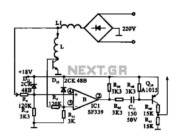
The minimum voltage required for this circuit is 8 volts, while the maximum voltage is 28 volts. It can be used to amplify audio signals in electronic devices such as radios, DVDs, MP4 players, and MP5 players. The circuit...
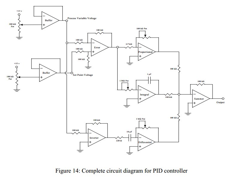
Convert a feedforward operational amplifier PID loop to C code. Assistance is needed for this conversion, as the process is unfamiliar. Input values can be obtained through an ADC, such as voltage or current, but coding a feedforward PID...
This is a successful vacuum tube project featuring a small amplifier where a 6V6GT output pentode is connected in triode mode, producing an output of approximately 4.5 watts. The project includes a single-ended audio amplifier with a resistive input...
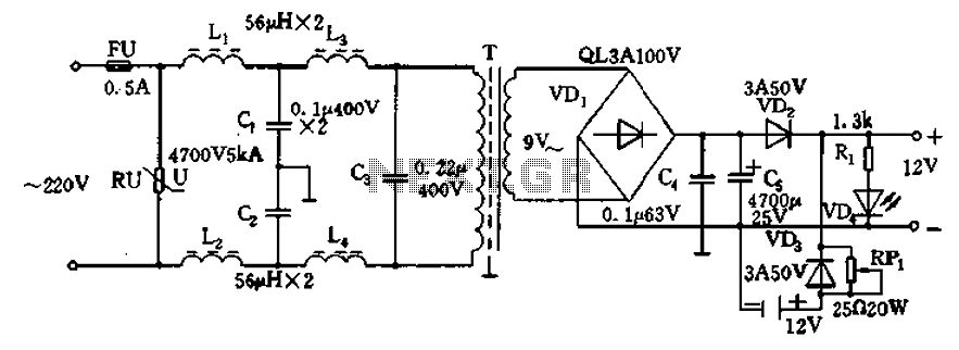
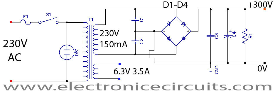
12V DC power supply circuit. A typical 12V DC power supply circuit includes a transformer that converts mains voltage to the required 12V AC output. It features a full-wave rectifier and a capacitor filter. The circuit typically incorporates a...